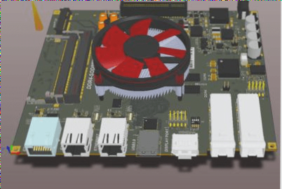
Recreating PCB Designs with Ease
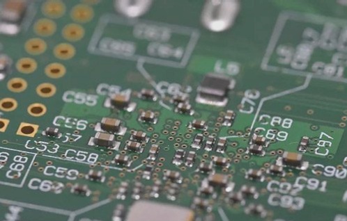
When it comes to recreating an existing PCB design, there are efficient methods that can simplify the process. One approach involves scanning the PCB at a high resolution, such as 600 DPI, and importing the image into design software. By adjusting the image opacity to around 50%, you can use it as a reference while laying out the new PCB design on top of it. Once the design is complete, you can remove the image without any hassle.
While tools like Adobe Illustrator offer this functionality, it’s worth noting that vector files are not typically used for manufacturing PCBs. However, there is no inherent limitation preventing their use, provided a standardized layering approach is established. For instance, separating the silkscreen layout, drill holes, and other elements onto distinct layers can streamline the manufacturing process.
Are you searching for PCB design software that supports this feature? Such software could eliminate the need for manual measurements when determining trace/pad dimensions, positioning, and shapes. This could significantly enhance the efficiency of your PCB design workflow.
Explore Advanced PCB Design Solutions
- Efficiently recreate existing PCB designs using high-resolution scanning techniques.
- Utilize design software with transparency settings to overlay new designs on scanned images.
- Consider standardized layering methods for organizing PCB design elements effectively.
- Discover PCB design software that streamlines the design process by automating measurements and layout tasks.