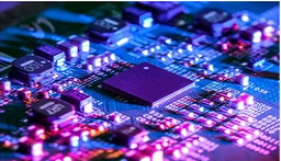
Advancements in ALV HDI Technology for PCB Manufacturing
As electronic devices such as smartphones, tablets, and wearables continue to shrink in size and increase in functionality, the PCB industry is facing the challenge of creating boards with higher layer counts and reduced thickness. With insulating layers now thinner than 50 μm, issues like decreased dimensional stability and electrical performance have arisen, particularly in signal impedance and insulation resistance. Additionally, the density of signal traces has grown, with trace widths now below 40 μm. Traditional subtractive methods struggle to fabricate such intricate traces, leading to the exploration of additive manufacturing techniques.
Recent Challenges and Solutions in ALV HDI PCB Technology
- Overview of ALV HDI Technology
Social media’s prominence has revolutionized communication through mobile devices, emphasizing the need for efficient corporate marketing strategies. The surge in data transmission volume, driven by enhanced functionalities and component miniaturization, underscores the rapid development of PCBs. Semiconductor technology, doubling every two years, is a key driver of this evolution.
Challenges in ALV HDI PCB Manufacturing
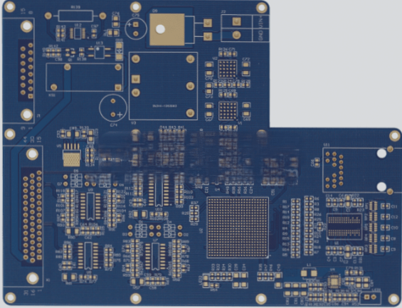
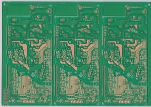
The production of miniaturized ALV HDI PCBs involves complex steps like multilayer lamination, laser drilling, imaging, etching, and electroplating. The key challenge lies in optimizing these processes for high-volume, reliable, and cost-effective production.
The Evolution of Micro-Hole Laser Technology
In response to decreasing component pin pitches, the PCB industry shifted to micro-hole technologies in the mid-1990s. Laser drilling emerged as the preferred method due to its flexibility, surpassing TEA CO2 and UV Nd:YAG lasers. Direct drilling through copper foil has become the primary method for producing blind microvias for inter-layer connections, although challenges like defects in micro blind holes persist.
Electroplating and Imaging Process
PCB Electroplating Process and ALV HDI Technology
- PCB electroplating process influenced by line width/spacing, insulating layer thickness, and final copper thickness
- In a 0.3 mm pitch BGA design, pad diameters are 150 μm, blind holes are 75 μm
- Challenges in producing fine circuits with existing subtractive methods
- ALV HDI Technology Summary
- Highlighting critical processes in producing layer interconnection PCBs
- Impact on costs and meeting current/future electronic packaging requirements
- Challenges in HDI PCBs: increasing functionality, size reduction, ultra-thin structures
- Efficient supply chain management, shortening prototype production cycles
- Accelerating market entry for products