Latest Advances in PCB Technologies
- With the introduction of new semi-additive technologies, trace widths in printed circuit boards (PCBs) can now be reduced to as low as 1.25 mils, allowing for increased circuit assembly density.
- The industry’s most commonly used subtractive PCB process offers a minimum wiring design tolerance of 0.5 mil, impacting impedance control in thinner wiring designs.
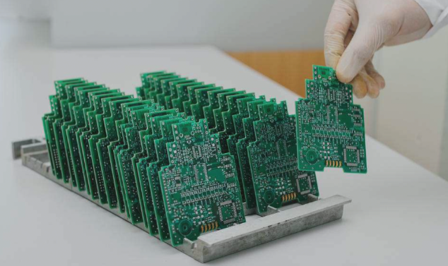
- PCB manufacturing initially involves covering one or both sides with a copper-containing substrate material known as the core, leading to variations in insulation and mechanical properties.
Subtractive vs. Semi-Additive Methods
When comparing the subtractive and semi-additive methods in PCB manufacturing:
- The subtractive method involves etching copper in an acid bath to create a wiring design, while the semi-additive method laminates a substrate with a thin copper foil and utilizes photolithography for wiring design.
- Precise impedance control is crucial for high-speed digital systems and microwave applications, with the semi-additive method offering advantages in achieving near-vertical wiring designs.
Impedance Control and Circuit Assembly Density
Key points regarding impedance control and circuit assembly density in PCB manufacturing:
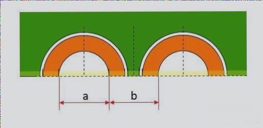
- Attaining a rectangular wiring design enhances predictability in impedance, leading to improved circuit assembly density and manufacturing yield.
- The semi-additive method allows for maintaining a wiring design width of 1.25 mils with controlled impedance, benefiting high-speed digital systems and microwave applications.