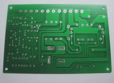
Essential PCB Layout and Routing Tips for Optimal Power Supply Circuit Design
Creating a robust power supply circuit hinges on a meticulously crafted PCB layout and routing strategy to ensure efficient signal transmission. The effectiveness of the circuit is intricately linked to the quality of the PCB design. In the realm of product development, numerous revisions often stem from PCB design challenges, particularly when extensive modifications are required post-initial design. Issues like improper placement of filter and power circuits, inadequate spacing, and suboptimal angle selections can result in significant near-field coupling noise. In such scenarios, repeated tweaks to the EMI filter may prove futile in mitigating noise transmission, necessitating a layout overhaul to enhance performance.
Key Recommendations for PCB Layout and Routing:
- Overall Layout of Power Supply: Prioritize the sequence of power input, surge protection circuit, EMI filter, and power supply module. Avoid U-shaped layouts that can lead to power leakage within high-frequency magnetic fields.
- EMI Filter Circuit Layout: Implement the Kelvin connection method for differential mode capacitance and ensure proper positioning of the Y capacitor for low-impedance grounding.
- Layout of Key Circuits and Voltage Movement Points: Minimize loop area in switching and rectifier circuits to reduce near-field radiation that may interfere with control signals.
- Layout of Magnetic Components: Perforate copper areas beneath high-frequency transformers and inductors to prevent noise coupling to signal traces.
- Control Circuit Layout: Separate power and control circuits to mitigate near-field interference and route grounds separately with a single-point ground.
- Drive Circuit Layout: Keep drive circuits near switching transistors to control loop area and minimize radiated noise.
- Primary-Side Capacitor Layout: Position filter capacitors close to the transformer and switching transistors to reduce common-mode loop area and noise current flow.
Enhancing Product Performance through Sound PCB Design Practices
By adhering to best practices and steering clear of common pitfalls in PCB layout and routing, product developers can significantly elevate the performance of their creations. Thoughtful consideration of layout intricacies and adherence to industry guidelines can pave the way for robust and efficient power supply circuits.
Essential Tips for PCB Layout and Routing in Power Supply Design
When designing a power supply, following fundamental guidelines for PCB layout and routing is crucial. Organizing the layout by circuit module can help you better grasp and retain these principles. By delving into this guide, you can enhance your knowledge of managing power EMI effectively.
If you require PCB manufacturing services, feel free to reach out to us. Contact us