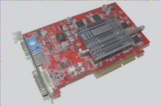
Designing RF Small Signal Amplifiers for Wireless Communication Systems
In wireless communication systems, amplifying weak radio frequency (RF) signals is crucial for ensuring reliable signal reception. RF small signal amplifier circuits are designed to not only amplify weak signals but also provide frequency selection capabilities to filter out interference signals. These circuits are categorized into narrow-band and wide-band amplifiers, each serving specific functions:
Narrow-Band Amplifiers:
- Employ active devices like transistors or integrated circuits for voltage gain
- Use LC resonant circuits, ceramic filters, quartz crystal filters, or surface acoustic wave (SAW) filters for frequency selection
Wide-Band Amplifiers:
- Amplify weak signals over a broad frequency range without distortion
- Require low lower cut-off frequency and high upper cut-off frequency
- Utilize transistors, field-effect transistors, or integrated circuits for voltage gain
RF Small Signal Frequency-Selective Amplifiers:
- Consist of active amplifier components and passive frequency-selective networks
- Active elements include transistors, field-effect transistors, or radio frequency integrated circuits
- Passive networks may include LC resonant circuits, SAW filters, ceramic filters, or crystal filters
Key Technical Parameters:
- Gain
- Passband
- Selectivity
- Linearity
- Noise figure
- Isolation
- Stability
Designing RF small signal amplifier circuits involves balancing various technical parameters like gain, passband, selectivity, and stability. Prioritizing these parameters based on specific PCB design requirements is essential for optimal circuit performance. Achieving a balanced compromise in the design process is crucial for the functionality of the amplifier in wireless communication systems.

Reducing Noise in RF PCB Small Signal Amplifiers
The output noise in an RF PCB small signal amplifier primarily originates from the input and the amplifier circuit itself. The noise generated by the amplifier has a significant impact on the transmitted signal, especially when dealing with weak signals. To minimize internal amplifier noise, it is crucial to select low-noise amplifying components during circuit design and manufacturing. Additionally, choosing the appropriate operating conditions, optimizing the circuit structure, and ensuring a proper PCB layout are key factors in reducing overall noise levels.
Latest Information: Recent advancements in RF PCB technology have led to the development of new low-noise amplifying components that further enhance signal quality and reduce interference. Engineers are now exploring innovative ways to integrate these components into circuit designs to achieve even lower noise levels.
If you have any questions about PCBs, please contact us at info@wellcircuits.com