The first time a buyer hears “solder mask,” it often sounds like a cosmetic choice—green versus black, matte versus glossy, maybe a branding decision. But anyone who has lived through a bad build knows the truth: solder mask is less about color and far more about manufacturing control.
I have seen projects where the BOM was perfect, placement was accurate, and the reflow profile was dialed in—yet the assembly still suffered bridging, inconsistent wetting, or field corrosion. When we dug into it, the root cause was rarely “the solder paste.” More often it was mask: unclear openings, missing dams between pads, or an assumption in CAD that did not survive Gerber export and CAM interpretation.
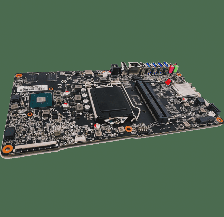
This article is written for engineers and procurement teams buying PCB fabrication and PCBA assembly who want fewer surprises. We will connect the “why” (reliability and yield) to the “how” (Gerber polarity, CAD workflows, and manufacturable rules). Along the way, you’ll see practical examples from KiCad, Altium, EAGLE/Fusion, and Allegro—and how to communicate clearly with a fabricator such as Well Circuits without turning the project into an email marathon.
1) What a Solder Mask Really Does (Beyond Color)
Solder mask (also called solder resist or soldering mask) is a thin dielectric polymer coating applied over copper on a PCB. On a solder mask PCB, it is applied everywhere except where you intentionally want exposed metal for soldering, probing, or special finishes.
Functional benefits that directly affect yield and reliability
- Controls solder wetting: it defines where solder can flow and helps prevent solder bridging, especially on fine-pitch parts.
- Protects copper from oxidation and corrosion: exposed copper ages quickly in humid or contaminated environments; mask helps stabilize long-term performance.
- Improves insulation and reduces contamination pathways: mask blocks residues and moisture from settling on copper features.
- Adds mechanical reinforcement: it can reduce pad lifting risk during thermal cycling, rework, or localized stress.
- Supports electrical robustness: as an insulating coating, it contributes to dielectric strength—though it should not be treated as your only safety barrier.
The key takeaway: solder mask is a process-control layer. If the openings are wrong, your assembly process becomes less predictable, and your risk (scrap, rework, latent failures) increases.
2) Solder Mask Materials and Application Processes: What Changes on the Factory Floor
Material selection and application method are usually driven by cost, throughput, and the resolution your design needs. Understanding the common options helps you ask better questions when comparing suppliers.
Common solder mask systems in production
- Liquid epoxy solder mask: typically applied by silkscreen. Cost-effective, but not ideal for very fine features.
- LPI solder mask (liquid photoimageable): applied by screen or spray, then exposed and developed to create accurate openings. This is a mainstream choice for modern SMT boards.
- Dry film solder mask (DFSM): vacuum-laminated film, then imaged and developed. Often chosen when high-resolution definition is required.
After imaging and development, curing hardens the coating. Many systems use thermal curing; some formulations support UV curing. Regardless of chemistry, the manufacturing target is consistent: precise and repeatable mask openings and stable adhesion after curing.
If you want fewer assembly surprises, treat solder mask as a controlled manufacturing feature, not a default checkbox. A good fabrication partner will emphasize process control at imaging, development, and curing because small deviations can translate into big assembly problems.
3) Technical Parameters That Matter: Openings, Dams, Alignment, and Thickness
Most solder mask disputes are not philosophical. They are dimensional. Designers think in ideal geometry; factories think in tolerances and process windows. The more your design rules align with real capability, the fewer “CAM modifications” happen without your awareness.
Key terms you should align on
- Solder mask opening: the intentional exposed area in the mask where copper/pad is solderable.
- Solder mask expansion: how much larger (or smaller) the opening is than the copper pad outline.
- Mask dam / web: the strip of solder mask between adjacent openings that helps block bridging.
- Registration: alignment accuracy between solder mask and copper layers.
- Minimum solder mask sliver: the smallest manufacturable dam/web that can reliably survive fabrication and registration tolerances.
When these are not specified—or when CAD defaults conflict with footprint overrides—your solder mask output can become unpredictable, especially on fine pitch, high-density layouts.
Table 1: Practical solder mask design and process parameters (typical ranges)
The values below are typical industry ranges used in many production environments. Always confirm final limits with your chosen fabricator and your specific stack-up and feature density.
| Parameter | What It Controls | Typical Range | Risk If Too Aggressive |
|---|---|---|---|
| Solder mask expansion (per side) | How much larger the opening is than the pad | 0.00–0.10 mm | Openings overlap; dams disappear; bridging risk rises |
| Minimum solder mask sliver (dam/web) | Smallest strip of mask between openings | 0.05–0.10 mm (advanced processes may go lower) | Mask dams get removed in CAM or fail in production |
| Mask-to-copper registration tolerance | Alignment error budget between copper and mask | ±0.05–±0.10 mm | Pad edges partially covered or copper unintentionally exposed |
| Solder mask thickness (cured) | Barrier protection, robustness vs. topography | 10–30 µm (varies by system and topography) | Too thin: weak protection; too thick: poor definition near fine pitch |
| Silk-to-solder mask clearance | Prevents legend ink printing onto openings | 0.10–0.20 mm | Silkscreen clipped by solder mask or ink contamination near pads |
4) Negative vs. Positive Solder Mask Gerbers: The Most Common “Fab Got It Wrong” Moment
One of the fastest ways a project gets derailed is when a buyer reviews a solder mask Gerber and concludes, “This is inverted.” In reality, solder mask outputs are frequently treated as negative layers: they define openings (where mask is absent) rather than drawing the entire coated area.
This convention is common because it is efficient. It is easier to specify a set of openings than to define a full-board polygon and subtract thousands of pads. The problem is human: a negative mask can look “wrong” if you expect the file to show ink coverage explicitly.
When reviewing solder mask Gerbers, shift your mindset: do the openings look correct? Pads, test points, special exposed copper areas, and via tenting decisions should appear exactly as intended.
5) KiCad: Why Mask Layers Look “Empty” and What That Actually Means
KiCad outputs solder mask data using a negative convention: the F.Mask and B.Mask layers define openings only. The software assumes the board is coated by default, and your mask layers carve out the places where copper must remain exposed.
This leads to a classic confusion: if your bottom side has no SMD pads or no intentional openings, the B.Mask Gerber may look empty. That is not automatically an error. It can simply mean: “no openings are required on that side; apply full coverage.”
Where things go wrong is when an automated submission portal rejects an “empty” mask file, or when a vendor expects a different convention. The fix is rarely to redraw your PCB; it is to confirm conventions early and ensure mask layers are present, named correctly, and interpreted correctly in CAM.
6) Verifying Solder Mask Openings in KiCad Before You Release Gerbers
If there is one habit that prevents expensive back-and-forth, it is this: validate mask openings by checking the actual Gerbers, not only the board view.
What to check (and in what order)
- Export Gerbers including F.Mask and B.Mask.
- Open Gerbers in an independent viewer and confirm openings exist where you expect exposed copper.
- Use KiCad’s 3D Viewer as a sanity check, but do not treat it as the final authority for manufacturing output.
- Pay special attention to any “free copper areas” you want exposed (high-current solder points, chassis bonds, hand-solder zones). These must show clear mask openings.
In typical manufacturing flow, the mask Gerbers are authoritative. A fabricator will build to them. If openings are absent in F.Mask/B.Mask, the default result is: the copper gets coated, and later you discover “it won’t solder.”
7) KiCad DRC: “Solder Mask Aperture Bridges” and the Real Fix (Pad-Level Control)
KiCad’s DRC warning “front solder mask aperture bridges with different nets” appears when two neighboring openings overlap, eliminating the dam between pads. Even if copper is still isolated, assembly risk increases because there is no mask barrier to resist solder spread.
The most common cause is overly large solder mask expansion inherited from a footprint library. The best fix is almost always pad-level control, because that is where the problematic expansion is often defined.
Recommended pad-level workflow
- Open the footprint in the Footprint Editor.
- Select the pads that are colliding.
- Reduce the pad’s solder mask expansion until openings no longer touch.
- Re-run DRC and re-check the mask Gerbers.
Some teams set expansion to 0 for fine pitch and let the fabricator apply a safe offset during CAM, but this should be a deliberate choice, not an accident.
8) Controlling Fine-Pitch Mask Dams in KiCad: Priority Rules and Minimum Web Width
Missing solder mask dams are usually not a rendering issue. They are the predictable result of rule priority plus a manufacturability constraint.
Two mechanics that matter
- Clearance priority: pad settings override footprint defaults, which override board/project settings. If you adjust a board-level rule and nothing changes, check pad overrides.
- Minimum web (minimum mask width): after generating openings, KiCad evaluates the remaining strip of mask between them. If it is below your minimum, KiCad removes it, merging openings.
A simple calculation explains many surprises. If pad-to-pad spacing is 0.20 mm, and each pad has 0.08 mm expansion per side, the remaining dam is 0.20 − 0.08 − 0.08 = 0.04 mm. If your minimum web is larger than 0.04 mm, the dam will be removed by design.
In buyer terms: if your board relies on ultra-thin dams to prevent bridging, you need a fabricator who can reliably register mask at that density—and you need your CAD rules to match that capability.
9) A Practical “How-To”: Removing Solder Mask from Existing Tracks in KiCad v8
Sometimes you intentionally want exposed copper on a trace: high-current solder reinforcement, a localized soldering area, or inspection access. In KiCad v8, you can create a solder mask opening over existing tracks by generating a polygon on the mask layer.
Workflow: “Create polygon from selection”
- Set F.Mask as the active layer in the Appearance panel.
- Select the target track segments on F.Cu (test with one segment first).
- Right-click and choose Create from Selection → Create polygon from selection.
- Select Create bounding hull.
- Set Gap = 0 and Line width = 0 for a tight opening.
- Ensure Delete source object is unchecked.
- Edit polygon properties (press E) and set style to Filled.
Once filled, the polygon defines a continuous mask clearance over the copper. This is a controlled way to expose exactly what you intend, while keeping the rest protected.
10) Altium: Why “Keep-Out” Does Not Create Solder Mask Openings
In Altium Designer, keep-outs are constraints for routing/placement and DRC behavior. They do not automatically generate solder mask apertures in Gerbers. A common mistake is placing keep-out objects on a solder mask layer and expecting exposed copper in fabrication—then receiving boards where everything is covered except normal pads.
What works in Altium
- Draw real primitives (regions, fills, polygons, tracks/lines) on the Top/Bottom Solder layers.
- Do not mark them as keep-outs.
- Verify in 3D view, then verify again by inspecting exported Gerbers in an independent viewer.
Think like CAM: if it is not in the mask Gerber as an opening, it does not exist for manufacturing.
11) Fusion/EAGLE: The “Mask Limit” That Overrides Via Tenting
Via tenting is a small decision that can have large consequences near BGAs and fine-pitch parts. In Fusion Electronics (EAGLE), two controls interact: the via’s own Solder Mask property (Auto/Off/Offset) and a global Mask Limit setting under design preferences.
The trap is that Mask Limit can override per-via settings during Gerber export. Vias may look tented in 3D, but still export with openings—creating solder-wicking risk during reflow.
Reliable fix
- Set Mask Limit to a very large value (commonly 999) to effectively disable the threshold behavior.
- Then confirm via-level settings drive the final tenting/opening decision.
- Verify the exported solder mask Gerbers—do not rely only on 3D view.
This single configuration change can prevent avoidable assembly yield loss around high-density packages.
12) Allegro: Missing Mask Openings Often Start in the Padstack
When a shop reports missing solder mask openings on pads or PTH features from an Allegro design, the cause is frequently simple: the padstack has no solder mask aperture defined. Allegro does not always infer mask openings from copper the way designers expect; definitions must exist in the padstack.
Fixing it correctly
- Go to Tools → Padstack → Modify Design Padstack.
- Select an affected pad, then Edit to open the Padstack Editor.
- Add or correct the solder mask opening/expansion definition.
- Update to Design, regenerate outputs, and re-check mask Gerbers.
- Update the library padstack too, so future projects inherit correct behavior.
From a buyer’s perspective, library consistency matters. It reduces manufacturing questions and lowers the chance that one board in a family behaves differently from the rest.
13) Zero Clearance vs. Explicit Clearances: When to Let the Fabricator Decide
Many PCB buyers are surprised to learn how often fabricators adjust solder mask in CAM. Even if your CAD says “0 expansion,” the shop may apply an internal offset to protect yield—especially to maintain a safe dam width or compensate for registration tolerances.
Using zero clearance can be reasonable when your design is not sensitive and you trust the shop’s defaults. But on fine pitch, relying on blanket CAM rules can create unintended outcomes: merged openings, lost dams, or unexpected copper exposure.
A balanced approach that avoids surprises
- Use explicit rules on fine-pitch and high-density footprints where dams matter.
- Use 0 clearance only when the design has comfortable spacing and you have confirmed the shop’s default solder mask expansion behavior.
- Ask the fabricator what they do in CAM when your design violates their minimum mask dam limits.
Table 2: Decision guide for solder mask expansion strategy
This table summarizes practical choices buyers and engineers make, and what to expect from manufacturing.
| Design Situation | Recommended Strategy | Why It Works | What to Confirm with the Fabricator |
|---|---|---|---|
| Comfortable pad spacing, low density | Use simple/global rules; consider 0 clearance | Process window is forgiving; CAM tweaks won’t change function | Default mask expansion and registration tolerance |
| 0.5 mm pitch QFN/QFP, tight dams | Set explicit pad/footprint-level solder mask expansion | Predictable dam formation; fewer CAM “helpful” changes | Minimum solder mask sliver and how violations are handled |
| BGA with nearby vias / thermal vias | Define via tenting rules explicitly; verify Gerbers | Prevents solder wicking and voiding risks | Via tenting capability, plug/fill options if needed |
| Special exposed copper areas (tinning points, bonds) | Create explicit mask openings on mask layers | Avoids “it looked exposed in CAD but not in Gerber” | Any restrictions on large openings and surface finish impacts |
14) Peelable Solder Mask: When Temporary Protection Beats Permanent Rules
Permanent solder mask is not always enough. During wave soldering, selective soldering, rework, or aggressive cleaning, you may need temporary protection over areas that must stay pristine: contacts, gold fingers, card-edge features, or “no solder” mechanical interfaces.
Peelable solder mask is a temporary coating—often latex-like—that is applied only where needed, cured, and later peeled away. It is designed to tolerate soldering temperatures and resist flux and common cleaning fluids, then remove cleanly without abrasive scraping.
Where peelable mask is commonly used
- Gold fingers and edge connectors
- Test contacts that must remain uncontaminated
- Areas prone to wave solder splash
- Regions that must remain clean before conformal coating steps
For high-mix production, peelable mask can be a practical process aid when geometry alone cannot protect “no solder” areas.
15) Preventing Peelable Mask Breakage: Dispensing Angle, Bead Thickness, and Cure
Peelable mask failures are often blamed on the material, but the most common root cause is technique. Holding the applicator at 90° and dragging tends to push uncured material into plated holes and vias. Once cured, that plug can “snap” during peeling, leaving fragments behind and creating cleanup headaches.
What works better in practice
- Dispense with the bottle mostly upright but tilted around 60°, encouraging a thicker blanket rather than a thin string.
- Avoid forcing material into holes; a thicker bead improves mechanical integrity during peeling.
- Ensure full cure before exposing boards to extreme soldering temperatures to reduce brittleness and tearing.
These are small process controls, but they dramatically change operator experience and post-solder cleanup time.
16) Solder Mask Is Not a “Guaranteed Insulator” for Mechanical Contact
Solder mask is electrically insulating, but it is not intended to be the only barrier when a metal shield, connector shell, or chassis part can press against the PCB. If your product relies on solder mask to prevent a hard short under mechanical stress, you are betting on a coating not designed or qualified for that job.
Practical alternatives when you need durable isolation
- Conformal coating (applied intentionally for insulation and environmental protection)
- UV-curable adhesive as a localized insulating layer where contact is expected
- Kapton tape as a fast, reliable barrier under metal parts
- Physical insulating sheets or barriers designed into the enclosure
This distinction matters in procurement reviews because a “mask-only” assumption can turn into an intermittent field failure that is expensive to diagnose.
17) A Buyer-Focused Quality Checklist: What to Ask Before You Place a PCB/PCBA Order
Buyers rarely lose sleep over the chemistry of solder resist. They lose sleep over schedule risk, yield, and “will this batch match the last one?” A good supplier will translate solder mask decisions into predictable manufacturing outcomes.
Table 3: Solder mask quality control checkpoints (what good looks like)
This table maps solder mask risk to practical controls that you can ask about during supplier selection or NPI kickoff.
| Checkpoint | What Can Go Wrong | What to Ask / Verify | Why It Matters to Buyers |
|---|---|---|---|
| Gerber interpretation (polarity and conventions) | Openings inverted, “empty” mask misread, unexpected coverage | Confirm negative/positive handling; confirm file naming and required layers | Prevents respins and schedule slips caused by avoidable misunderstandings |
| Minimum solder mask dam capability | Dams removed; openings merged; bridging risk increases | Ask for minimum solder mask sliver spec and registration tolerance | Protects assembly yield on fine-pitch designs |
| Mask expansion defaults and CAM edits | Factory modifies openings without design intent | Ask what they do when expansion is 0 or when dams violate minimum | Improves predictability and reduces “surprises in mass production” |
| Imaging, development, and curing controls | Poor definition, adhesion issues, inconsistent openings | Ask about process control points and inspection (e.g., AOI for mask alignment if available) | Consistency across batches reduces rework and warranty risk |
| Pre-production review and DFM feedback | Hidden issues discovered after boards arrive | Request DFM checks for fine pitch, via tenting, special openings | DFM feedback is cheaper than schedule recovery |
18) Bringing It All Together: A Simple Workflow That Prevents Most Solder Mask Surprises
If you want a practical routine that works across CAD tools and suppliers, keep it simple and repeatable:
- Decide intent: which copper must be exposed, which vias must be tented, where dams are critical.
- Implement in CAD: create real mask openings on mask layers (not routing keep-outs) and set pad-level rules for fine pitch.
- Export Gerbers and inspect: verify F.Mask/B.Mask openings in an independent viewer.
- Align with the factory: confirm polarity conventions, minimum dam capability, and whether they will apply CAM expansion.
- Lock it for production: document mask assumptions in your release notes so future revisions don’t drift.
This is the difference between “we hope it’s fine” and “we can predict what will be built.”
Conclusion: Treat Solder Mask Like a Manufacturing Interface, Not a Background Layer
Solder mask sits at the intersection of design intent and assembly reality. It protects copper, supports reliability, and—most importantly—controls solder behavior when it matters most: during reflow, wave, and rework. But it only does that job when openings, dams, and conventions are defined correctly and verified in the same language your fabricator uses: Gerbers.
If you are preparing a new build or troubleshooting yield issues, make solder mask part of your standard review checklist. Verify the mask Gerbers, confirm minimum dam capability, and avoid CAD “tricks” that do not translate into manufacturing data. This is one of the highest-leverage habits in PCB/PCBA procurement.
If you want a second set of eyes before release, consider requesting a DFM review focused on solder mask openings, fine-pitch dams, and via tenting. Teams working with Well Circuits often reduce turnaround time by uploading Gerbers early and clarifying mask conventions upfront. Request a quote or upload your Gerber files for a pre-check—it is usually faster (and cheaper) than finding out after the boards arrive.