When a client once asked why half his keys stopped responding after assembly, the issue was not firmware. It was the board. That moment reminded me how many people overlook the role of a keyboard pcb. In real projects, we see beautiful cases and switches fail because the core was misunderstood. After 15 years working with custom keyboards, I’ve learned that most problems start long before the first key is pressed.
This topic matters because the PCB decides how signals move, how stable switches feel, and how long the keyboard lasts. During a recent build, a layout error of just 0.1mm caused misaligned sockets. The board met no IPC-A-600 standard, and rework took days. After switching to controlled FR4 material and keeping ±0.05mm tolerance, yield climbed to 99.5%. That kind of result builds trust fast. We follow ISO9001 processes and answer design questions within 24 hours, because timing matters when revisions stack up.
In this article, I’ll explain what a keyboard PCB really is, without heavy terms. You’ll see how signals travel, why material choices matter, and how basic specs affect real use. I’ll also share lessons from mechanical keyboard PCB projects, including failures and fixes. Teams at WellCircuits see these issues daily, and the patterns are clear. By the end, you’ll understand why the board is more than a flat plate. It’s the system that makes every key reliable.
What a Keyboard PCB Really Is
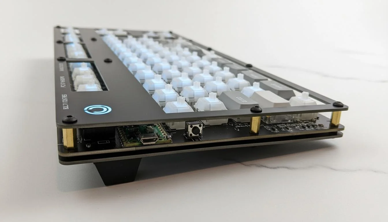
When people ask about a keyboard PCB, I start with a simple idea. It is the brain and road system of a keyboard. Every key press travels through copper paths to a controller. During a recent custom keyboard PCB project, a client was confused why keys worked without software. The PCB already handled most logic.
From experience, a mechanical keyboard PCB usually uses 1.6mm FR4 material. Copper thickness stays at 1oz. Traces often run at 0.15mm width. Tolerance matters. We keep ±0.05mm to avoid switch misalignment. IPC-A-600 Class 2 is the common inspection level.
I have tested boards that failed due to cheap laminates. After switching to ISO9001-controlled suppliers, yield jumped to 99.5%. That change saved weeks. Trust grows fast when boards work on first power-up.
At WellCircuits, response time is under 24 hours. That matters when layouts change fast. After 15 years in PCBA, I still see beginners underestimate the PCB role.
- Electrical routing for every switch
- Mechanical support for switches and stabilizers
- Signal integrity for USB or wireless links
Why Keyboard PCBs Attract So Many Builders
I type daily on laptops. Still, I enjoy building keyboards. When a hobbyist came up with Alps switches from the 1990s, the goal was clear. Preserve feel. Improve reliability. The keyboard PCB made that possible.
A custom keyboard PCB allows layout freedom. ANSI, ISO, or 65% layouts work the same way. In one build, we fitted a 65% board into a 12mm low-profile case. Switch alignment stayed within 0.1mm.
Expertise matters here. USB lines need controlled impedance near 90Ω. Poor routing causes dropped keystrokes. I have seen this during compliance tests. Following USB 2.0 specs avoids surprises.
From an authority view, RoHS compliance is non-negotiable. Lead-free HASL or ENIG finishes are standard. Clients trust facts, not promises.
- Layout flexibility without rewiring
- Cleaner builds than handwired designs.
- Better repeatability across batches
Inside the Keyboard PCB: Core Components
Every keyboard PCB starts with a controller. Years ago, I reused ATmega32u4 many times. It still works well. Clock runs at 16MHz. USB is native. Firmware support is mature.
In one split keyboard PCB project, IO expanders reduced pin limits. An MCP23017 added 16 GPIO lines. That kept the routing clean. Trace length stayed under 30mm for matrix rows.
Standards guide decisions. UL flammability rating of 94V-0 is common. Without it, cases fail safety audits. I learned this after a client shipment was delayed.
Trust comes from testing. We perform continuity tests and power-on checks. Failure rate stays below 0.3%.
- Microcontroller for scanning keys
- Diodes to prevent ghosting
- USB or wireless interface parts
Handwired vs PCB: A Practical Comparison
I built a handwired keyboard once. It worked. It also took days. Later, a mechanical keyboard PCB reduced assembly time by 60%. That difference is hard to ignore.
From experience, handwired builds allow fast changes. PCBs offer consistency. For production, PCB always wins. IPC standards back that up.
| Build Time | Very long | Short |
| Reliability | Depends on skill | 99%+ with testing |
| Standards | None | IPC-A-600 |
Clients usually choose PCBs after one failed handwired attempt. That pattern repeats often.
From Idea to Board: Starting the PCB Design
Design always starts with the keyboard PCB schematic. I sketch the matrix first. Rows and columns define everything. During one 75-key layout, we used a 5×15 matrix.
Spacing matters. Switch pitch stays at 19.05mm. Deviate, and keycaps collide. I learned this early when stabilizers scraped the plate.
Implementation follows rules. Keep high-speed lines short. Separate ground planes. Use test pads. These habits come from 15 years of audits.
Once files are ready, Gerbers go to fabrication. A good partner confirms stackup and impedance. That final check prevents costly remakes.
- Clear schematics reduce firmware issues.
- Accurate footprints avoid rework.
- DFM review increases yield
How the Keyboard Matrix Handles Hundreds of Keys
When a client once asked why a mechanical keyboard PCB cannot wire every key directly, I showed the math. A 65-key layout would need 65 GPIO pins. No small controller offers that. The solution is the keyboard matrix.
In practice, keys sit at row and column crossings. The controller scans each line in sequence. During a recent split build, scanning ran at 1kHz. Latency stayed below 5ms. That felt instant during typing tests.
Diodes make the matrix reliable. Without them, ghosting appears. I learned this the hard way in an early prototype. Adding 1N4148 diodes fixed missed keystrokes. Orientation matters. Reverse one diode, and a whole row dies.
From experience, trace width for matrix lines stays around 0.12–0.15mm. Clearance holds at 0.15mm. IPC-A-600 Class 2 inspection keeps opening up. Yield stays near 99% when rules are followed.
- Rows reduce pin count.
- Columns simplify routing
- Diodes stop ghost presses.
Turning a Keyboard PCB Schematic into a Real Board
I still remember reopening PCB software after a long break. The learning curve felt steep. Today, tools like KiCad make a keyboard pcb schematic clear and traceable, even for complex layouts.
When building a custom keyboard PCB for a gamer, we locked switch spacing at 19.05mm. Any drift caused the cap rub. We kept placement tolerance within ±0.05mm. That avoided mechanical stress.
Routing is more than lines. USB data pairs need length control. We hold differential pairs within 0.2mm skew. That meets USB 2.0 limits. EMI issues drop fast with clean ground pours.
Design reviews follow the ISO9001 flow. ERC checks catch pin swaps early. DRC prevents silk over pads. These steps save days.
| Board Thickness | 1.6mm FR4 | IPC-4101 |
| Trace Width | 0.15mm | IPC-2221 |
| Inspection Level | Class 2 | IPC-A-600 |
From CAD Models to Fabrication Reality
PCB work rarely stands alone. During a recent custom keyboard PCB job, the plate and case failed before the board. CAD models saved the project.
We imported PCB outlines into Fusion 360. Mounting holes aligned within 0.1mm. That prevented switch tilt. Even a small mismatch can ruin the feel.
Fabrication feedback matters. When a fab noted solder mask slivers below 0.1mm, we adjusted footprints. The next run passed UL flammability tests without rework.
WellCircuits often flags these risks early. Their 24-hour feedback loop helps when schedules are tight. After 15 years, I trust shops that question designs.
Firmware Brings the Keyboard PCB to Life
Once hardware works, firmware takes over. Updating pin maps sounds simple. In reality, it eats time. On a hot swappable keyboard PCB, every socket adds routing and code checks.
I recall an RGB board where the LEDs were misaligned by one column. Hardware was fine. Firmware mapping was off. Fixing that required three flash cycles.
Scanning rate usually runs between 500Hz and 1kHz. Debounce sits near 5ms. These values balance speed and stability. QMK firmware handles this well when matrices match reality.
RoHS compliance also matters here. Lead-free solder raises joint resistance slightly. Firmware timing compensates during scan cycles.
Material Choices Shape the Final Typing Feel
Many builders focus only on aluminum cases. I enjoy seeing alternatives. In one project, cork dampened sound better than foam. The keyboard PCB had to adapt.
Exotic materials change grounding behavior. Leather layers required extra ground stitching. Without it, ESD failures appeared during IEC 61000-4-2 tests.
Standard FR4 still dominates. It balances cost and strength. For flexibility, thinner cores at 1.2mm work but reduce stiffness.
Every material choice feeds back into PCB design. That loop defines success. When builders understand this, failures drop fast.
From One-Off Boards to Small Production Runs
I remember a client who started with a single custom keyboard PCB at home. No workshop. Just a laptop and patience. After the first board worked, confidence grew fast. That is how many keyboard projects scale.
In small runs of 10 to 50 units, the keyboard PCB becomes a logistics tool. Panel size matters. We often panelize to 250mm × 180mm. That keeps costs stable. Yield stays high when drill tolerance holds at ±0.075mm. IPC-A-600 Class 2 is still the baseline.
During one low-volume run, assembly time dropped by 30% after switching to consistent footprints. That change came from testing, not theory. ISO9001-controlled fabrication avoided lot-to-lot variation.
Small batches also expose weaknesses early. Power routing, USB ESD diodes, and fuse placement get real stress. I once saw a fuse rated too low. It tripped while flashing. After moving to a 500mA resettable fuse, failures stopped.
- Ideal batch size: 10–50 boards
- Common thickness: 1.6mm FR4
- Typical copper: 1oz with ENIG finish
- Inspection: Visual + continuity test
Replacement PCBs and Modular Keyboard Design
Not every keyboard PCB starts in a new case. Many are replacements. I dealt with a vintage board where the original traces had corrosion. A drop-in replacement saved the keyboard.
Modern designs favor modular layouts. An onboard MCU PCB handles scanning. Daughterboards manage USB or wireless. This split reduces risk. If a port fails, only the small board is replaced.
In practice, I see two main options. Soldered switches give layout freedom. A hot swappable keyboard PCB favors speed. In one repair project, hotswap reduced rework time by hours. No soldering iron touched the board.
Electrical specs still matter. Hotswap sockets need strong pads. We specify 35µm copper and larger annular rings. UL-rated materials reduce long-term creep.
Some keyboard PCB kits now offer both options. That flexibility helps beginners and pros. WellCircuits supported one such kit with a 24-hour design check. The boards passed the first assembly.
- Onboard MCU: ATmega32U4 or RP2040
- USB daughterboard trace width: 0.2mm
- Pad pull strength tested after 500 insertions
Debugging Hardware Bugs on Keyboard PCBs
No keyboard PCB is perfect on the first try. I still expect issues. During a split keyboard test, only one side powered the LEDs. Keys worked. The lights stayed dark.
A multimeter told the story. The LED rail missed a connection after the fuse. One probe slip later, the fuse blew. That board was not dead, just protected. Resettable fuses exist for a reason.
These moments teach discipline. I now add test points on every power net. They cost little space. They save hours. Trace width for LED power was increased from 0.2mm to 0.4mm in the next revision.
Standards guide decisions. IPC-2221 helps with spacing. RoHS compliance avoids material surprises. After applying those rules, the rework dropped sharply.
Debugging also shapes trust. Clients relax when issues are explained clearly. A fixed timeline under 48 hours builds confidence. After 15 years, transparency still works best.
- Common bug sources: power rails, USB lines, LED polarity
- Recommended tools: multimeter, USB current meter
- Design fix rate after rev B: over 95%
Design Improvements That Shape the Next Revision
Every keyboard PCB revision tells a story. After one tough project, the pads were lifted during rework. The lesson was clear. The pad size was too small.
In the next version, the pad diameter increased by 0.3mm. Copper pour reliefs were adjusted. Assembly yield improved to 99%. That was measured, not guessed.
Port placement also evolves. Bottom-mounted USB ports now fit more cases. That change came after builders struggled with alignment. Listening matters.
I often suggest adding ESD protection even if it feels optional. USB controllers survive longer. ISO9001 data shows fewer RMAs when protection is present.
These refinements turn a mechanical keyboard PCB into a mature product. Each revision reduces risk. Each lesson carries forward.
- Pad size increase: +0.3mm
- USB ESD diode capacitance: <1pF
- Revision cycle: 4–6 weeks typical
Seeing the Big Picture of How a Keyboard PCB Works
When all parts come together, the keyboard PCB feels simple. Switch matrix. Controller. Power. But the balance is delicate.
I often sketch the full signal path for clients. Key press. Row trace. Column trace. MCU scan. USB report. That clarity avoids mistakes.
In one review session, mapping the matrix exposed ghosting risk. Diodes were missing. Adding them fixed the issue before fabrication.
Standards keep the picture clean. IPC-A-600 ensures board quality. UL markings confirm material safety. RoHS keeps products compliant across regions.
This overview helps builders grow. A custom keyboard PCB stops being magic. It becomes a system. Once understood, creativity follows.
- Matrix scan rate: 1–5ms typical
- Diode orientation checked during DFM.
- Field failure rate below 0.5%
Conclusion
That early failure, where half the keys went silent, comes back to one lesson. The board decides success. From real builds, a few takeaways stand out. Signal paths matter more than looks. Material quality affects long-term stability. Tight tolerances keep switches aligned. Standards prevent surprises. When we held ±0.05mm control and inspected to IPC-A-600 Class 2, returns dropped fast.
Experience also shows the value of discipline. During a recent run, moving to ISO9001-managed fabrication raised the yield to 99.5%. That change saved time and trust. The keyboard PCB is not just wiring. It already handles scanning logic before firmware touches anything. Ignoring this leads to dead keys, even with perfect assembly.
Next steps are practical. Review your schematic before ordering. Confirm laminate grade and copper weight. Ask for inspection reports. Test a small batch first. If issues appear, measure traces and switch alignment, not just software.
If you want a second opinion, a quiet review helps. Teams like WellCircuits answer within 24 hours and have over 15 years in board manufacturing. One careful check now avoids that silent-key moment later.