Advanced Techniques in PCB Manufacturing
1. Evolution of PCB Technology
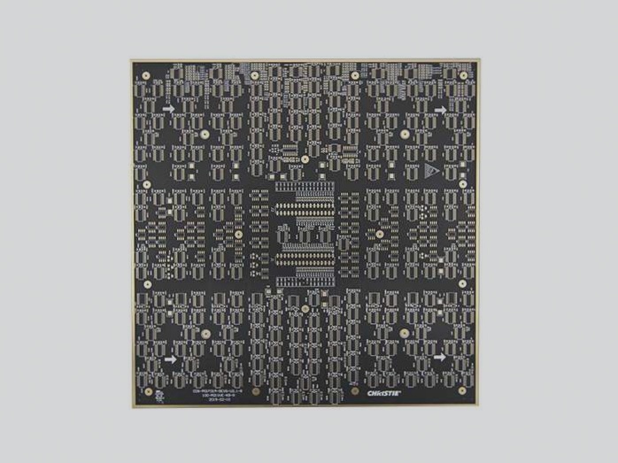
With the rapid advancement of microelectronics, the manufacturing of printed circuit boards (PCBs) has progressed towards multi-layered structures, stack-ups, functionalization, and integration. This evolution has led to the design of circuit patterns with intricate features such as tiny holes, narrow spacing, and thin wires, making PCB manufacturing more complex.
2. Challenges in High-Density PCBs
High-density PCBs, particularly those with through holes exceeding an aspect ratio of 5:1 and deep blind holes in buildup boards, pose challenges for traditional vertical electroplating processes. The current distribution within these holes often results in uneven copper deposition, leading to quality issues and potential wastage.
3. Innovations in Electroplating
To address quality concerns, advancements in electroplating focus on optimizing current distribution and additives. Techniques such as low current densities, high-quality additives, and controlled agitation aim to enhance copper deposition uniformity, especially in high aspect ratio PCBs.
4. Horizontal Electroplating Technology
As aspect ratios increase, traditional methods may become ineffective, necessitating the adoption of horizontal electroplating. This novel approach builds upon vertical electroplating principles, emphasizing compatibility, power supply enhancements, and improved dispersibility for superior plating results.
5. Electroplating Process Fundamentals
- Both horizontal and vertical electroplating require cathode and anode electrodes.
- Electrification initiates electrode reactions, leading to metal ion movement and deposition.
- Metal deposition involves ion diffusion, dehydration, and lattice integration at the cathode.
6. Electric Double Layer Theory
The electric double layer theory explains the interaction between electrodes and plating solutions. It elucidates the arrangement of cations near the cathode and the formation of Helmholtz outer layers, crucial for electroplating processes.
7. Future Prospects
Continued research into electroplating methods promises enhanced PCB manufacturing capabilities, paving the way for high-quality, reliable interconnect solutions in modern electronic devices.
Understanding the Diffusion Layer in PCB Electroplating
When it comes to PCB electroplating, the diffusion layer plays a crucial role in the plating process. Let’s delve into some key points:
1. Diffusion Layer Composition
- The diffusion layer, located farther from the cathode, experiences convection effects leading to a higher concentration of cations compared to anions.
- Due to electrostatic forces and thermal motion, the cation arrangement in the diffusion layer is less orderly than in the Helmholtz outer layer.
2. Thickness and Flow Rate Relationship
The thickness of the diffusion layer is inversely proportional to the flow rate of the plating solution. Higher flow rates result in thinner diffusion layers, while lower flow rates lead to thicker diffusion layers.
3. Transport Mechanisms
- Copper ions in the diffusion layer move towards the outer Helmholtz layer through diffusion and ion migration.
- In the main plating solution layer, copper ions reach the cathode surface via convection and ion migration.
4. Convection Effects
Convection in the plating solution is induced by various factors such as mechanical stirring, pump stirring, and temperature differences. This convection impacts the uniformity of the plating solution concentration.
5. Flow Interface Layer
Close to the solid electrode surface, the flow of the plating solution slows down significantly due to frictional resistance. This creates a flow interface layer with a thickness approximately ten times that of the diffusion layer, minimizing the influence of convection on ion transport.