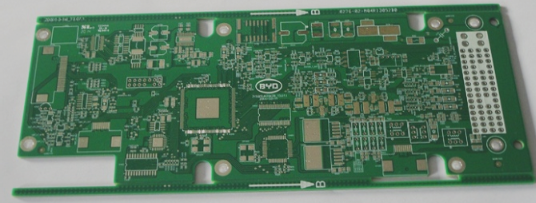
PCB Layout Design Principles
- Arrange all components on the same side of the circuit board, except for dense top components like chip resistors and capacitors.
- Components should be placed on a grid, parallel or perpendicular to each other, without overlap, for an organized layout.
- Maintain a minimum distance of 1 mm between adjacent land patterns of different components.
- Keep a distance of at least 2 mm from the edge of the circuit board, with a rectangular shape preferred.
Layout Design Guidelines
- Position functional circuit units according to signal flow for efficient circulation.
- Use core components as the center and arrange others uniformly and compactly around them.
Quality Control of PCB Circuit Boards
PCB proofing is essential before mass production to ensure quality. It involves independent testing and strict control measures.
What is PCB Proofing?
PCB proofing is a test run of circuit board designs before mass production, allowing for quality assessment and adjustments.
Ensuring Quality
Quality PCB proofing involves higher standards, faster delivery, and better performance. Manufacturers like Shenchuang Electronics prioritize independent testing for quality assurance.
Quality Check Process
Each PCB undergoes careful inspection during drilling and copper sinking processes to maintain quality standards.
Quality Manufacturing
Robust quality control measures are implemented during production to meet timeliness and cost targets, ensuring high-quality PCBs.
Quality Usage
After production, PCBs are tested for quality and performance to guarantee reliability in electronic products.