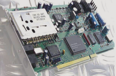
DFM in PCB Manufacturing Process
General Requirements
- This standard establishes general requirements for effective communication between CAD and CAM in PCB design and manufacturing.
- PCB companies prioritize design drawings and documentation as the basis for production.
PCB Material
- Substrate: The PCB substrate typically consists of FR4, which includes epoxy glass cloth copper clad laminate for single-layer boards.
- Copper Foil:
- Copper foil must be over 99.9% electrolytic copper.
- The thickness of copper foil on the surface of the finished double-layer board should be ≥35 μm (1 OZ).
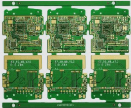
PCB Structure, Dimensions, and Tolerances
Structure
- All design elements relevant to the PCB must be clearly indicated in the design drawings.
- Long slot holes or hollow areas should be outlined using the Mechanical 1 layer in the design drawing.
Board Thickness Tolerance
Overall Dimension Tolerance
The external dimensions of the PCB must adhere to the specifications outlined in the design drawings with a tolerance of ±0.2mm (excluding V-CUT products).
Flatness (Warpage) Tolerance
The PCB’s flatness must meet the specifications provided in the design drawings.
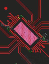
Printed Wires and Pads
Layout
- The layout, line width, and spacing of printed wires and pads should conform to the design drawings.
- Adjustments will be made based on process requirements to enhance reliability.
- Recommended specifications for vias (VIA) and line spacing.
- Minimum drilling tool, line spacing, and line width standards.
Wire Width Tolerance
The internal control standard for printed wire width tolerance is ±15%.
Grid Processing
- Design large copper areas in a grid pattern to prevent blistering and PCB bending.
- Recommended grid spacing and line width.
Treatment of Thermal Pads
Considerations for large-area grounding to reduce heat dispersion and virtual solder joints.
Aperture (HOLE)
Definition of Metallization (PTH) and Non-Metallization (NPTH).
Non-Metallized Holes in PCB Design
- Our company follows specific methods for non-metallized holes in PCB designs:
- When customers opt for non-metallized properties for mounting holes in Protel99se or use Keep Out layers, we treat these as non-metallized holes.
- If NPTH is placed near a hole or a customer explicitly requires a non-metallized aperture, we comply accordingly.
Metallized Holes and Via Holes
- All component holes, mounting holes, and via holes are typically metallized in PCB designs.
- Aperture sizes have a tolerance of ±3mil (0.08mm), while VIA holes have a positive tolerance within +3mil (0.08mm).
Thickness and Roughness
- The copper-plated layer in metallized holes is generally no less than 20μm in thickness, with a minimum of 18μm.
- PTH hole wall roughness is controlled to be ≤ 32μm.
PIN Hole and SLOT Hole Design
- Positioning pin holes have a minimum diameter of 0.9mm, with three arranged in a triangular formation.
- SLOT holes should be designed using the Mechanical 1 layer or connecting holes of the same size for alignment.
- For shielding purposes, a SLOT hole diameter of at least 1.2mm is recommended.
Solder Mask Guidelines
- All PCB surfaces, except pads, MARK points, and test points, should be coated with a solder mask.
- Graphics on the solder mask layer should indicate areas for tinning based on customer requirements.
- Solder mask adhesion must meet Class 2 requirements per US IPC-A-600F standards.
DFM Technical Requirements
The outlined technical requirements serve as a reference for customers during PCB design to enhance communication between CAD and CAM processes, aiming for efficient Design for Manufacturability (DFM) and cost reduction.