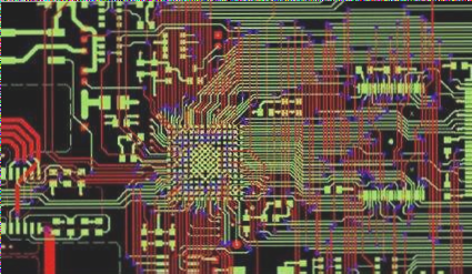
Key Principles for Multilayer PCB Layout and Wiring
Designers must adhere to specific principles when laying out and wiring multilayer printed circuit boards:
- Component Printed Traces Spacing: When determining the spacing between different networks on a PCB, designers should consider electrical insulation, manufacturing processes, and component trace dimensions. For example, if a chip component has a pin spacing of 8 mil, the clearance constraint should not exceed 6 mil to ensure proper design.
- Manufacturing Capabilities: Designers should set spacing rules based on the manufacturer’s production capabilities to ensure manufacturability.
- Electrical Insulation: It is crucial to address electrical insulation issues, especially when dealing with significant potential differences between components or networks. The typical clearance safety voltage is 200 V/mm or 5.08 V/mil, emphasizing the importance of maintaining safe distances, especially when high-voltage and low-voltage circuits coexist on the same board.
If you require further adjustments or have any questions, feel free to reach out!