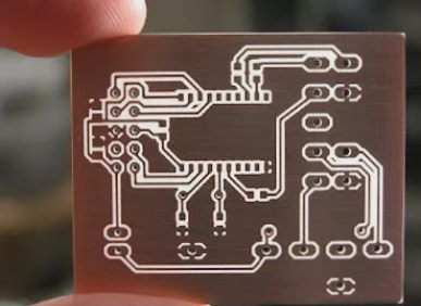
Key Points for Effective PCB Board Design
- Design Direction: When designing a PCB board, it is crucial to establish a logical direction for components to prevent interference. Consider factors like input/output, AC/DC, signal strength, frequency, and voltage levels. Avoid circular layouts to maintain isolation.
- Grounding Points: Selecting the right grounding points is essential for a well-functioning PCB. Ensure a common ground and merge multiple ground wires to the main ground to minimize interference.
- Power Filter/Decoupling Capacitors: Place filtering and decoupling capacitors close to the components needing them to optimize performance and address grounding issues.
- Line Diameter and Hole Size: Pay attention to the size of lines and holes, especially for high-voltage and high-frequency applications. Wide ground wires with ample copper area enhance grounding effectiveness.
- Number of Vias, Solder Joints, and Line Density: Minimize vias to streamline production and prevent soldering issues. Control line density to avoid solder joint merging and ensure welding quality.
Mastering these key points in PCB board design enhances production efficiency, product quality, and cost-effectiveness. WellCircuits Limited specializes in high-precision circuit boards, offering double-sided, multi-layer, impedance-controlled, and thick copper boards tailored to various customer requirements, including HDI, backplanes, and rigid-flex boards.


