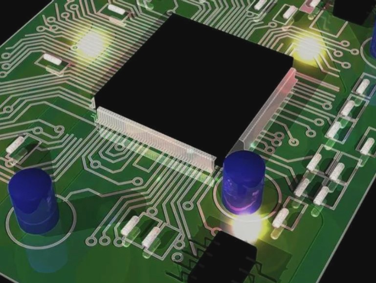
Evolution of ATE Load Boards in the Semiconductor Industry
Years ago, “ate load board” was the common term for automatic test equipment (ATE) PCBs in the semiconductor industry. However, the industry now refers to them as “device interface boards (DIBs)” or “processor interface boards (HIBs).”
Rapid Turnaround and High-Quality Evaluation
- Chip manufacturers demand rapid turnaround and high-quality evaluation for their advanced products, surpassing previous test board standards.
- Manufacturing timeframes have decreased from two to three months to six to eight weeks due to the faster production of chips.
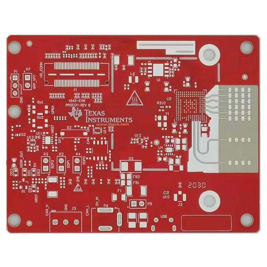
Designing High-Quality ATE PCBs
ATE PCB suppliers now ensure a quicker delivery timeline of six to eight weeks, offering additional services like wafer testing and inspection. Expertise in design knowledge is crucial for creating high-quality ATE PCBs, considering factors like BGA packaging and ball spacing reduction.
Ensuring Quality and Accuracy
- Strict adherence to manufacturing standards is essential for accurate test board results.
- Placement of bypass capacitors and voltage limitations are critical, especially with the design of 30 to 50 ply boards.
Adapting to Technological Advances
Technological advancements in BGA spacing and wiring widths require ATE PCB designers to adjust their layout and wiring techniques. Precision in routing, differential pair widths, and impedance matching are vital to meet chip manufacturer requirements and ensure test result accuracy.