PCB Via Types and Design Considerations for International Electronics Manufacturers

Understanding PCB Vias: Essential Connections in Modern Circuit Board Design
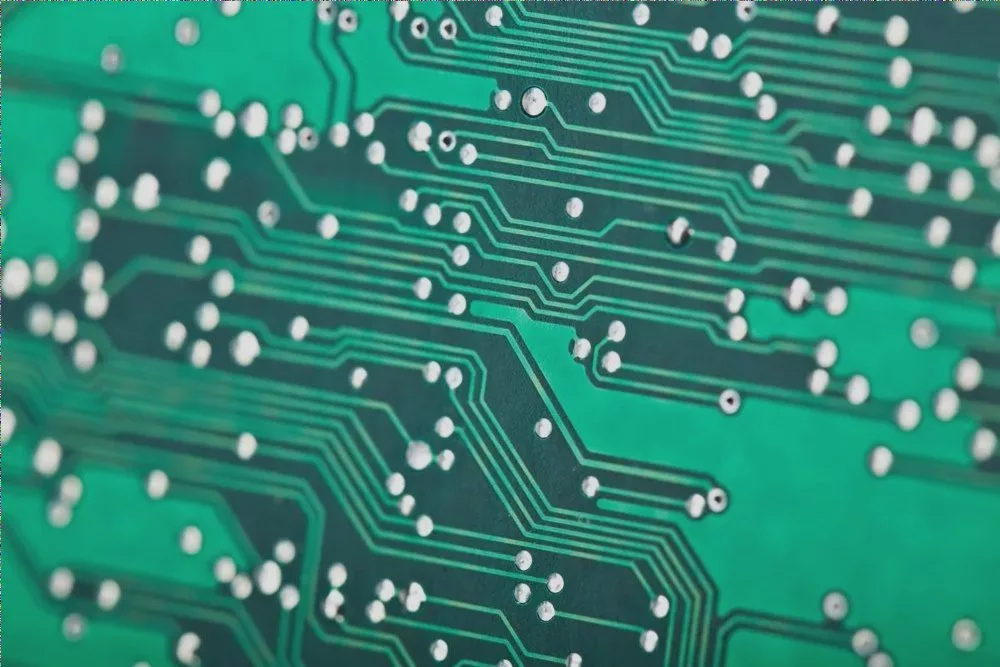
As electronic products continue to shrink in size while growing in complexity, multi-layer PCB boards have become the standard in international electronics manufacturing. Among their critical components, vias serve as the vital pathways connecting isolated copper layers, enabling sophisticated circuit designs in compact spaces.
The Three Fundamental Via Types for Global PCB Applications
When sourcing PCB manufacturing in China or other global markets, understanding these core via types is essential:
- Through-hole vias – Penetrate the entire board from top to bottom
- Blind vias – Connect an outer layer to adjacent inner layers
- Buried vias – Link inner layers without reaching the surface
Through-Hole Vias: The Standard for Reliable PCB Connections
As the most common via type in international PCB manufacturing, through-holes come in two variants:
“Plated Through Holes (PTH) feature copper-plated walls for electrical conductivity, while Non-Plated Through Holes (NPTH) serve mechanical purposes like board mounting or test fixture positioning.”
Key considerations when choosing through-hole PCB manufacturers:
- PTH diameters must accommodate component leads
- NPTH typically requires larger diameters for mechanical stability
- Cost-effective solution for most standard PCB applications
Advanced Via Solutions for High-Density PCB Designs
Blind Vias: Space-Saving Connections for Complex Boards
Ideal for HDI PCB manufacturing, blind vias connect surface layers to adjacent inner layers without penetrating the entire board. These are particularly valuable when working with:
- High-density component placement
- Miniaturized electronic devices
- Complex multi-layer PCB designs

Buried Vias: The Hidden Solution for Inner-Layer Connections
For electronics manufacturers requiring maximum routing space, buried vias offer:
- Connections between internal layers only
- No surface visibility, preserving outer layer space
- Enhanced reliability for complex circuit designs
Special Via Design Considerations for International Buyers
Via-in-Pad Technology: Optimizing Space in Modern PCB Layouts
With the rise of BGA package PCBs, via-in-pad design has become crucial for:
- Miniaturized component placement
- High-density interconnect (HDI) applications
- Space-constrained electronic devices
However, international buyers should be aware of potential solder wicking issues that can affect reliability.

Via Covering Options: Ensuring PCB Reliability
When evaluating PCB manufacturers in China or other global suppliers, consider these via covering techniques:
- Tenting vias – Solder mask coverage prevents solder migration
- Plugged vias – Partial filling with insulating material
- Filled vias – Complete via filling for planar surfaces
These solutions address common quality concerns like solder leakage and short circuits during reflow processes.

Selecting the Right PCB Manufacturer for Your Via Requirements
When sourcing international PCB production, consider these critical factors:
- Manufacturer expertise in your required via technologies
- Capability to handle complex multi-layer designs
- Quality control measures for via reliability
- Experience with your specific industry applications
As a leading PCB manufacturer with global export experience, Wellcircuits offers comprehensive via solutions tailored to your project’s technical requirements and quality standards.