Testing and Inspecting PCB Components: A Complete Guide
All you need to know about how to test PCB
When investing in PCB and PCB assembly, ensuring their longevity is crucial. Learn how to test PCB to diagnose and resolve issues efficiently.
What components of PCB do you need to analyze during PCB inspection?
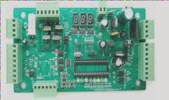
Understanding the PCB manufacturing process and the importance of its components is essential for effective PCB testing. Components like capacitors, diodes, resistors, fuses, and transistors play vital roles in circuit development.
- Capacitors
- Diodes
- Resistors
- Fuses
- Transistors etc.
Inspecting these components is key to identifying and resolving PCB abnormalities.
General steps included in the inspection of PCB
Testing PCB involves using tools like a multimeter, soldering gun, and magnifying glass. Before delving into specific testing methods, follow these general steps:
Spot visual defects inspection
Prioritize visual inspection of PCB components like resistors, capacitors, and ICs. Look for cracks, burnt copper wires, or broken traces using a magnifying glass to identify and rectify issues.

Check the power system of the circuit
After visual inspection, assess the power supply system using a multimeter to ensure voltage levels are within expected ranges. Replace fuses if necessary and troubleshoot components causing current overflow.
Inspection of input and output system
Examine the input and output systems of the PCB to identify any irregularities affecting circuit performance.
Methods for Testing PCB Designs
-
Burn-in Testing
Burn-in testing is effective in detecting PCB failures but can be damaging due to high current flow.
This test involves passing current through components for over 50 hours, which can harm copper wires and fuses.
-
Flying Probe Testing
Flying probe testing is a cost-effective method to detect PCB layer problems using needle probes.
It is suitable for checking short circuits, capacitance, resistance, and diode issues.
-
Automated Optical Inspection
This method utilizes optical lenses and cameras to identify flaws in PCB designs.
It compares captured images with the expected board to detect and address design deficiencies.
-
In-Circuit Testing
This method offers comprehensive PCB testing using fixed probes to ensure solder connection integrity.
It provides effective testing coverage and is relatively inexpensive.
-
X-Ray Inspection
X-ray inspection allows deep scanning of PCBs to identify internal defects not visible during visual inspection.
It is particularly useful for pinpointing issues within inner chip layers of the PCB.
-
Functional Testing
Professionals use functional testing to ensure PCB compatibility with the design and electronic device functionality.
It helps in identifying and correcting design flaws before product launch.
-
Boundary Scan
Boundary scan is a modern technique to test PCB assembly functionality and connections with other electronics.
It verifies the connections of ICs with input and output plugs using physical probes.
Conclusion
Essential Steps for PCB Testing
Understanding how to test a PCB involves knowing which components require testing and the specific steps to follow. There are various methods available for PCB testing that can help ensure the accuracy and functionality of your circuit board.