Key Points of PCB Layout Design
- Today’s switching regulators and power supplies are becoming more compact and powerful, presenting challenges for designers.
- Higher switching frequencies are making PCB board design more complex.
- PCB layout plays a crucial role in the success of switching power supply designs.
- Design software like Webench can assist in component selection and optimization.
- Efficiency is a key factor, with considerations for input-output pressure differences.
- Choosing the right switching frequency is essential to avoid layout problems.
- Attention to current paths and di/dt effects is crucial for minimizing interference.
- Output capacitor connections should be wide and short to handle high current flow effectively.
For more information on PCB layout design and optimizing switching regulators, visit Wellcircuits.
Optimizing PCB Layout for High Current Applications
When designing PCB layouts for high current applications, it is crucial to consider the routing of wires and the placement of components. Traditional layouts that route wires from Vout and ground to capacitors may not be the most effective approach. Instead, connecting the output and ground directly to the capacitor terminals can help to mitigate issues related to large alternating currents.
One common misconception is the use of a ground plane on “Layer 2” to connect all grounds. However, this method may lead to ground bounce, especially in scenarios where different components have varying current flows. To address this, creating a star node for high current ground conductors on the input and output sides can help maintain a stable ground reference.
It is essential to keep ground wires short and thick to minimize interference and noise. High impedance nodes, such as the IC’s feedback pin, require special attention to ensure signal integrity. By optimizing the wiring method and reducing open board areas, the likelihood of noise interference can be minimized.
Key Considerations for PCB Layout:
- Connect output and ground directly to capacitor terminals
- Avoid ground bounce by creating star nodes for high current ground conductors
- Keep ground wires short and thick to reduce interference
- Pay special attention to high impedance nodes like the IC’s feedback pin
- Optimize wiring method to minimize open board areas and noise interference
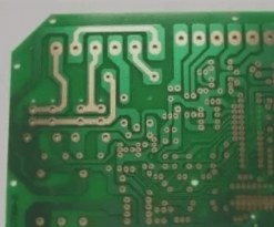
Practical Sample Analysis:
For practical applications, ensure that the wiring method for components like the resistor divider is optimized to prevent open areas that can act as receiving antennas for interference. By routing wires effectively and reducing open board areas, the overall performance and reliability of the PCB layout can be enhanced.
PCB Layout Design Tips for Switching Power Supply
- Pay attention to the space near CIN
- Ensure ground point of CIN capacitor is directly connected to diode anode
- Avoid shortening wire inside “power ground”
- Optimize positioning of FET[SW] to minimize wire length
- Keep an eye on resistor divider (FB1-FB2) proximity to IC
- Connect FB2 to independent ground plane
- Ground pins of IC should be treated similarly
- Use vias to connect “signal” ground to ground plane
- Connect “power” ground to GND pin using vias
- Prevent ground bounce on “signal” ground
- Follow layout design rules for smoother PCB design
- Take time to carefully plan PCB layout design for efficient troubleshooting
By implementing these simple rules in your PCB layout design for a switching power supply, you can ensure smoother operation and easier troubleshooting in the future.