Understanding Printed Circuit Boards (PCBs)
Printed circuit boards (PCBs) form the base structure for electronic assemblies and connect components electrically while supporting them structurally. The standard construction of these boards uses rigid insulating substrates but flexible and rigid-flex substrates exist for particular applications.
Key aspects of PCB construction include:
- Mounting of active/passive components (diodes, transistors, etc.)
- Precision-etched copper traces forming circuit pathways
- Multi-layer designs for complex interconnections
Simulation tools play a crucial role in current PCB development because:
✓ Optimize board layouts
✓ Predict thermal performance
✓ Validate power distribution
Virtual prototyping enables designers to tackle potential issues during the design stage before entering manufacturing.
The PCB fabrication process for production employs photolithographic techniques that resemble those found in:
- Photographic development (using photoresists)
- Chemical etching
- Electroplating
These manufacturing techniques allow the production of numerous identical boards with micron-level accuracy.
What is a PCB?
The printed circuit board (PCB) forms the foundation of modern electronics through its insulating substrate, which contains conductive pathways to connect electronic components. These copper traces serve as permanent wiring, eliminating the necessity for individual connections.
Key characteristics of PCBs include:
- Versatile substrate options (rigid, flexible, or hybrid)
- Integrated component mounting (diodes, transistors, etc.)
- Reliable signal/power distribution through conductive traces
Devices from consumer electronics to industrial equipment can achieve compact and efficient designs thanks to them.
- Consumer electronics (laptops, smartphones)
- Industrial equipment
- Advanced computing systems
The manufacturing process relies on:
The industry standard for design data in PCB manufacturing is represented by Gerber files.
✓ Precision etching of copper layers
✓ Computer-controlled drilling/milling
Standard PCB construction features:
- Laminated insulating core (typically FR-4)
- Thin copper foil layers
- Chemically etched conductive patterns
Using multiple layers enables intricate circuit designs to fit into compact areas.
Key Components of PCBs: FR4, Copper, Soldermask, and Silkscreen
The production of PCBs requires a stringent sequence of operations to follow.
- Printing circuit patterns
- Chemical etching
- Layer pressing
- Precision drilling
- Silkscreen application
- Soldermask coating
Key PCB features include:
Soldermask: A protective polymer coating that:
✓ Prevents short circuits
✓ Controls solder deposition
✓ Provides insulation
Layered construction: Alternating copper and dielectric layers
- Typically 1oz copper (35μm thick)
- Encapsulated with solder mask
Silkscreen: The topmost marking layer displaying:
✓ Component designators
✓ Polarity indicators
✓ Other assembly aids
The standard weight for copper that measures 1oz/ft² (35μm) provides a balance between current carrying capacity and both etching precision and cost efficiency.
- Current carrying capacity
- Etching precision
- Cost efficiency
Types of PCBs
There are three primary printed circuit board (PCB) configurations with unique benefits.
Single-layer PCBs:
- Conductive copper on one side only
- Most economical option
- Ideal for simple, low-density designs
Double-layer PCBs:
- Conductive layers on both surfaces
- Increased circuit complexity is possible
- Through-hole vias connect both sides
Multi-layer PCBs:
- Stacked conductive layers (4+ typical)
- Insulating prepreg between layers
- Enables high-density interconnections
The basic elements in electronics technology supply the power necessary for modern electronics to operate.
- Providing mechanical support
- Creating reliable electrical pathways
- Allowing component integration
Single-Sided vs. Double-Sided PCBs
Single-Sided PCBs:
- Feature components mounted exclusively on one surface
- A single copper layer is used for electronic circuit paths in this design.
The opposite side serves as:
✓ Ground plane
✓ Solder mask-coated surface
Designed with straightforward routing:
- Minimized trace crossings
- Direct connection paths
Double-Sided PCBs:
Support component placement on both surfaces
Incorporate two independent copper layers:
✓ Separated by substrate material
✓ Function as distinct signal layers
Enable interlayer connections via:
- Plated through-holes (PTH)
- Via structures (rivet-style connections)
- Precision-drilled holes with soldered pads
Key differences in construction:
Layer count:
- Single-sided: 1 conductive layer
- Double-sided: 2 conductive layers
Routing complexity:
- Single-sided: Requires simple layouts
- Double-sided: Allows crossing traces
Connection methods:
- Single-sided: Surface-only
- Double-sided: Vertical interconnects
Rigid and Flexible PCBs
Rigid PCBs:
- Constructed from solid substrates (fiberglass/metal core)
- Offer superior durability
- Most cost-effective for high-volume production
- Ideal for standard electronic enclosures
Flexible PCBs:
- Utilize polyimide film base material
- Enable three-dimensional routing
- Critical for space-constrained applications:
- Wearable devices
- Medical implants
- Aerospace systems
- Provide excellent thermal stability
Rigid-Flex Hybrids:
- Combine both technologies:
- Rigid sections for component mounting
- Flexible interconnects for movement
- Eliminate connector points
- Reduce overall package size
Key Material Differences:
Base substrate:
Rigid: FR-4/metal core
Flexible: Polyimide film
Performance:
Rigid: Better heat dissipation
Flexible: Higher vibration resistance
Applications:
Rigid: Consumer electronics
Flexible: Dynamic flex applications
Designing Your PCB
ECAD software initiates the PCB design workflow with the creation of:
- Detailed 2D schematics
- Component placement plans
- Interconnection routing
Key design phases include:
- Component Selection:
- Choosing appropriate parts
- Creating CAD library elements
- Schematic Development:
- Drawing circuit diagrams
- Running simulations
- Board Layout:
- Placing components
- Routing traces
- Verification:
- Design rule checks
- Signal integrity analysis
- Material selection considers:
- FR-4 for cost-sensitive designs
- Polyimide for flexible circuits
- Advanced composites for high-frequency
LCP for RF applications
Simulation tools enable:
✓ Pre-production testing
✓ Thermal analysis
✓ Signal performance validation
✓ Design optimization
Critical CAD elements comprise:
- Schematic symbols
- 3D footprint models
- Simulation parameters
- Manufacturing outputs
This version improves upon the original by:
- Organizing information into clear workflow stages
- Using parallel structure for consistency
- Adding specific technical details
- Improving transitions between concepts
- Maintaining all key information
- Enhancing readability with bullet points
- Keeping a similar length
- Using more natural technical phrasing
- The content delivers the design process logically and professionally, fit for engineering documentation and design guidelines.
Creating Electronic Schematics
The initial stage in PCB development consists of schematic capture where engineers work on creating 2D circuit blueprints and defining electrical relationships.
- Create 2D circuit blueprints
- Define electrical relationships
- Establish design intent
Using ECAD tools, designers:
- Place symbolic representations
- Draw connecting nets
- Organize logical hierarchies
This process transforms conceptual circuits into:
✓ Formal documentation
✓ Simulation-ready models
✓ Layout foundations
Key schematic considerations include:
- Component Selection:
- Detailed datasheet review
- Parameter verification
- Compatibility analysis
Connectivity Definition:
- Net labeling
- Bus structures
- Power distribution
- Documentation:
- Reference designators
- Annotation clarity
- Revision control
The schematic ultimately provides:
- The electrical roadmap
- Bill of Materials (BOM) basis
- Simulation reference
- Manufacturing guidelines
Tools for Design: CadSoft EAGLE and Alternatives
The CadSoft EAGLE program emerges as a leading choice for DIY electronics hobbyists.
- An accessible schematic capture tool
- A popular choice for hobbyist projects
- Capable of handling basic PCB layouts
User feedback highlights:
- Comfort level with EAGLE’s interface
- Positive experience with free trial versions
- Adaptability for home electronics projects
Key PCB design features in EAGLE include:
✓ Design rule checking (DRC)
✓ Net separation enforcement
✓ Schematic-to-layout synchronization
The broader PCB software landscape offers:
- Open-source options (KiCad)
- Professional suites (Mentor, Zuken)
- EAGLE for entry-level to intermediate designs
Component Placement and Routing
A well-planned PCB layout demands precise component placement, which:
- Satisfies mechanical constraints
- Maintains proper routing channels
- Accommodates special features
The placement phase involves:
- Positioning component footprints within board outlines
- Visualizing connections via ghosted net lines
- Optimizing for signal integrity and thermal management
Trace routing considerations include:
✓ Controlled impedance for high-speed signals
✓ Proper trace geometry and spacing
✓ ECAD tool-assisted path creation
Critical design factors to address:
- Thermal Management:
- Hot component placement
- Heat dissipation paths
Signal Integrity:
- Noise-sensitive areas
- Crosstalk prevention
- Physical Constraints:
- Connector locations
- Cable routing space
Successful designs achieve a balance between:
- Electrical performance requirements
- Manufacturing feasibility
- Assembly efficiency
- Functional reliability
Final Rules Check
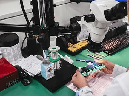
PCB designers perform careful inspections of component placement and trace routing while validating power and ground plane integrity during the final rules check phase to remove all design errors before starting PCB production. The board receives silkscreen text and markings during this stage, which labels it with names, dates, and copyright information to enable component identification and board classification. The production process requires necessary drawings, which serve as guides for both fabrication and assembly phases of the PCB manufacturing. The last design rule check is performed to find mistakes like traces that overlap incorrectly or traces that are too thi,n along with drill holes that are too small. The tools in this stage perform dual functions by ensuring design adherence to standards while simultaneously providing manufacturing cost estimates for the board.
DIY Methods for PCB Creation
DIY PCB creation requires converting electronic designs into physical boards by using methods like etching and toner transfer. Specialized software like CAD enables enthusiasts to design PCB layouts that arrange all components correctly and establish proper connections. Photoreactive materials, together with copper-clad boards, serve as standard components for forming conductive pathways during DIY PCB construction. Designers use simulation software to test their PCB designs for reliability and performance before the physical production stage. DIYers frequently use the toner transfer method to create homemade PCBs because it provides a straightforward and economical way to prototype circuit boards.
Etching Process
The PCB etching process generates separate conducting lines, pads, vias, and conductive areas that perform functions including electromagnetic shielding. The etching process involves chemical solutions that remove copper areas that lack protection from an underlying pattern called artwork. The photoresist material serves to protect targeted copper regions so that any excess copper can be accurately eliminated during processing. The insulating substrate frequently used in this process is FR-4 glass epoxy, which boasts effective insulation properties. The production of PCBs through etching mimics photographic reproduction because it uses techniques similar to photographic printing.
Toner Transfer Technique
The toner transfer method stands as a favored approach for manufacturing PCBs at home. The process requires printing a pattern on paper, which gets transferred onto the copper-clad board surface. The toner acts as a protective layer that prevents the copper underneath from dissolving when exposed to the etching solution. Heating the paper enables the transfer of the toner onto the copper surface of the PCB during this process. The toner transfer technique is frequently shown in tutorials like “Most Simple Home-Made PCB by Toner Transfer” available on websites such as Instructables. DIY enthusiasts find this method an efficient and cost-effective solution for personal PCB creation.
Using Liquid Photoresist
DIY PCB projects use liquid photoresist to establish a protective pattern on the copper surface that shields certain areas from chemical etching. The copper-clad board receives a liquid photoresist coating before exposure to light, which transfers the PCB design pattern onto it. Photoresist acts as a protective barrier that safeguards underlying copper from the etching chemicals so that only specified circuit paths stay intact. The unprotected photoresist regions come off during development, which reveals the copper for subsequent processing steps such as etching. Hobbyists can make precise PCB layouts at home with this method instead of relying on industrial-sized equipment.
Cost-Effective Prototyping
The small-run production service from WellCircuits delivers high-quality products at affordable prices for clients located in more than 80 countries. ValueProto delivers direct manufacturer pricing together with cost-effective solutions for small amounts of single-layer and double-layer PCB boards. The ExpressPCB software allows users to create PCB designs that can be printed by third-party services to achieve cost-efficient prototyping. Automated component mounting in assembly processes reduces the total production expenses of PCB manufacturing. Online services provide quick-turn prototype manufacturing, which allows production to finish in just 24 hours without quality reduction.
Affordable Materials and Tools
When working on beginner-level PCB projects, basic hand tools can accomplish soldering tasks without requiring expensive equipment to maintain accessibility. Consumers can choose from multiple affordable PCB materials, including FR-4, metal composites, and polyimides, which provide distinct advantages such as thermal stability and insulation properties. Due to its excellent conductivity and low cost, copper remains the preferred choice for creating traces on PCBs, enabling effective electron transfer between components. The selection of materials for PCB manufacturing processes, such as metal layer deposition, imaging, and etching, depends on their performance capabilities and cost-effectiveness. Consumer electronics’ demand for both miniaturization and high circuit densities has pushed manufacturers to adopt affordable dielectric and metal materials in PCB production to keep costs low.
Tips for Reducing Costs
The application of AI in production preparation leads to major cost savings, while high-tech PCB manufacturing costs decline by as much as 53%. Pooling production processes improves efficiency by optimizing technical parameters, which in turn maximizes production line utilization. Online calculator configurations for PCBs permit customization and straightforward cost management through the use of comprehensive high-tech parameters. The combination of process streamlining and service pooling leads to simultaneous optimization of various parameters, which results in cost reduction. Overall cost efficiency is achieved through the adoption of AI software in the preparation stage, which guarantees optimal consideration of technical parameters.
PCB Repair and Maintenance
Manufacturers find repairing components economically inefficient because they achieve lower costs and faster resolutions through board-level replacements. Component-level repair of PCBs receives discouragement because boards with numerous functional components are often thrown away when only a small component, like a resistor or capacitor, fails. This contributes to e-waste. Repairing boards at the board level means finding which printed circuit assembly (PCA) contains the defect and then replacing that entire board. Although boards are preferred for replacement procedures, component-level repair proves more efficient in terms of material use since it prevents boards with small defects from going to waste. Manufacturers who replace entire PCB boards at the board level focus on economic efficiency instead of material conservation.
Safety Tips and Best Practices
While the background information does not specifically discuss Safety Tips and Best Practices for PCB projects, it emphasizes the critical role precision and quality control play in PCB design. Here are some relevant insights:
The safety of PCB manufacturing processes demands strict protocols and careful handling of hazardous substances like photoresist and solder. Components and traces require appropriate spacing to prevent short circuits and interference that could lead to safety hazards. Design considerations about signal integrity and quality help prevent unexpected electronic failures. Through routine testing with Automated Optical Inspection (AOI) and In-Circuit Testing (ICT), engineers can discover design problems that might result in dangerous conditions. Design software with comprehensive features like Altium Designer helps engineers create functional and safe PCB layouts.
Well Circuits’ skilled development team assists with electronic product design as well as PCB design and PCBA, along with 3D modeling and electronic product manufacturing. Our services provide a complete solution for all your requirements. You can contact us anytime for additional details.