PCB Reverse Engineering: Understanding the Process
Introduction to PCB Reverse Engineering
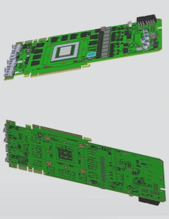
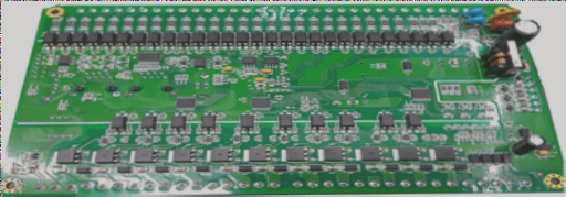
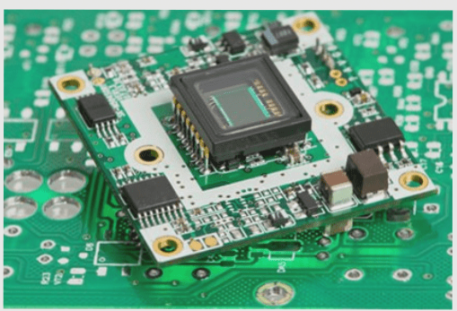
A Printed Circuit Board (PCB) is a fundamental component in electronics, providing support for electronic parts and facilitating electrical connections. The PCB fabrication process involves etching or printing circuit paths onto the board.
What is PCB Reverse Engineering?
PCB reverse engineering, also known as PCB copy, aims to replicate existing electronic products and their associated circuit boards. This process involves analyzing and reconstructing technical files, including PCB layouts, Bill of Materials (BOM), and schematics, to create a functional copy.
The Reverse Engineering Process
- Examine the original PCB carefully.
- Create technical documentation, including PCB files, BOM files, and schematics.
- Use the documents as blueprints for PCB manufacturing.
- Complete PCB fabrication, component soldering, flying probe testing, and circuit debugging.
- Reproduce the original PCB design for a functional copy.
Benefits of PCB Copying
PCB copying enables replication and improvement of electronic products, offering opportunities for secondary development and innovation. It allows for the extraction of technical data from existing products, facilitating the imitation and cloning of entire systems.
Evolution of PCB Copying
PCB copying has evolved beyond simple replication to include product secondary development and new product research and development. By analyzing existing product documentation, companies can evaluate new product feasibility, identify competitive advantages, and keep up with technological trends.
Rapid Upgrading and Development
PCB copying enables rapid upgrading and secondary development of electronic products. Engineers can modify technical files to enhance PCB design, add new functionalities, and redesign features for next-generation products. This process accelerates product iterations and improves functionality for a faster time-to-market.
Conclusion
PCB copy involves more than just cloning circuit boards; it drives innovation, product improvement, and competitive advantage in the electronics industry. By leveraging reverse engineering techniques, companies can stay ahead in the market and meet evolving consumer demands.
Challenges in PCB Manufacturing
Transitioning from a schematic diagram to a physical PCB board is a complex process that requires precision and expertise. While the theoretical principles of PCB design are well-known, the practical implementation poses significant engineering challenges. Many theoretical processes encounter difficulties in real-world execution, highlighting the importance of experience and attention to detail in PCB manufacturing.
Creating a high-quality, functional PCB involves more than just following a schematic – it requires a deep understanding of the manufacturing process and the ability to troubleshoot and optimize designs for real-world applications.
Stay updated with the latest advancements in PCB manufacturing to ensure your designs meet the highest standards of quality and functionality.