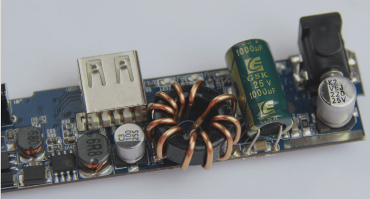
Circuit Board Edge Stamp Hole Design
When designing circuit boards, V-cut scoring and routing techniques are commonly used. However, another approach known as stamp hole design can also be employed.
- The term “stamp hole” refers to small holes strategically placed on the board, resembling perforated stamps. These holes allow for easy separation of the board using tools like pliers or manual breaking.
- Unlike scoring and routing methods, stamp hole design does not require specialized tools for separation. However, it may lead to burrs and uneven edges post-separation.
- Burrs and uneven edges from stamp hole separation can cause assembly issues and functional problems if not addressed properly.
- Separating stamp holes without standard tools can result in bending the board, leading to quality concerns like solder cracks and component damage.
The stamp hole design is crucial for circuit boards where V-cut is not feasible due to limitations. Poor stamp hole design can result in burrs that hinder assembly, requiring additional processing and potentially impacting product quality.
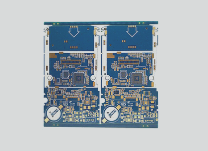
There are two distinct stamp hole designs, both featuring five small 1.0mm diameter stamp holes. The positioning of ribs plays a key role in determining the outcome post-separation.
In a poorly designed circuit board, burrs extending beyond the molding line require manual post-processing, leading to increased costs and contamination risks. On the other hand, a well-designed circuit board minimizes burrs within the molding line, reducing assembly interference.