Effective Ways to Test PCB Assembly
Introduction to PCBs
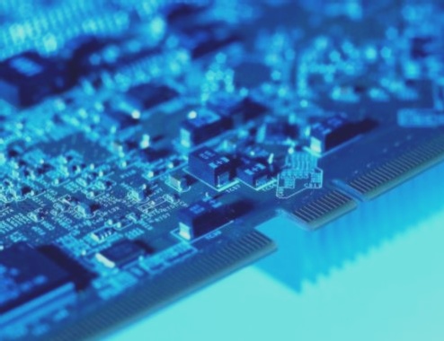
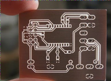
Printed circuit boards (PCBs) are non-conductive, multi-layer boards that serve as the foundation for connecting electronic components. They play a crucial role in supporting and connecting various electronic elements using conductive pathways etched onto a non-conductive substrate.
Importance of PCB Testing
Testing PCBs is essential to ensure they function efficiently. Here are the top methods used for PCB inspection:
1. Automated X-ray Inspection (AXI)
Automated X-ray inspection (AXI) is utilized to examine PCBs with components like BGA, CGA, and CSP. It uses X-rays to detect defects early in the assembly process, reducing costs and preventing issues during PCB assembly.
2. Automatic Laser Test Measurement (ALT)
Automatic laser test measurement (ALT) employs lasers for precise scanning and measurement of PCB components. It is effective in assessing solder position and quantity, although interference can impact accuracy.
3. Product Appearance Inspection (AOI)
Product appearance inspection (AOI) involves automated visual inspections of PCBs to identify critical and quality defects. This non-contact method uses high-resolution cameras or laser scanners to capture images for comparison and analysis.
Benefits of AOI
- Ensures PCB products function correctly
- Accurately checks complex board designs
- Detects manufacturing errors promptly
For more information on PCB testing, visit Well Circuits.
Automated Optical Inspection (AOI) in PCB Manufacturing
- AOI is an automated process where operators can set parameters for the scanner to check for errors.
Disadvantages of AOI System:
- AOI only detects PCB errors, not errors like glue or seal issues.
- Defect detection is not flexible and requires programming for each change.
- AOI does not detect new errors, only pre-programmed ones.
- Teams do not have access to data from the AOI system.
In-Circuit Test (ICT) for PCBs
In-Circuit Test (ICT) is a white box testing method where electrical probes check for errors like shorting and opening on a printed circuit board.
This test helps in identifying PCB failures during component repair, facilitating easy replacement of defective parts and ensuring accurate evaluation of the production process.
Limitations of In-Circuit Testing:
Parallel components may only be tested as a single component if they are of the same type.
Electrolytic components can only be tested for polarity in specific configurations.
Quality of electrical contacts cannot be tested without additional test points or specialized cables.
Some tests may not be possible if testing access is not provided by the PCB designer.
Why AOI Systems are Essential in PCB Assembly Testing
AOI systems are crucial for inspecting solder paste, solder joints, and component installation accuracy on PCBs.
X-ray systems are used for detailed inspections of components like large BGA parts with hidden solder joints.
Manufacturers utilize automated test systems for comprehensive testing, including ICT, flying probes, and cable scanning.
Functional testing simulates the operational behavior of a power supply to ensure proper manufacturing to specifications.
Challenges in Functional Testing:
Lack of a prepared test strategy and complete documentation package can lead to testing problems.
Inadequate Test Point Coverage:
Ensuring Effective PCB Testing
- Complete test point coverage is essential for ICT or flying probe testing.
- Test points should be adequately spaced for easy access by automatic test probes.
- Manually test probe points for network debugging and functional testing.
- Ensure test fixtures are up-to-date and accurate to avoid delays and increased costs.
- Using outdated components can hinder functional testing and verification processes.
Importance of Test Point Coverage
For successful ICT or flying probe testing, it is crucial to have complete test point coverage on the PCB. This means that every active net must be connected to a test point, either through dedicated design objects like surface mount pads or existing through-hole pins or vias.
Spacing of Test Points
Proper spacing between test points is essential to ensure easy access for automatic test probes. Maintain a gap of 50 mils between test points and other design objects, and 100 mils between test points and the board’s edge.
Manual Testing for Debugging
Technicians should manually test probe points for network debugging and functional testing purposes. These probe points, usually pads or holes, should be clearly marked on a wire mesh grid for easy access.
Importance of Up-to-Date Test Fixtures
Having the correct and current versions of test fixtures is crucial for efficient ICT processes. Outdated or incorrect fixtures can lead to delays and increased costs, especially when modifications are needed.
Impact of Outdated Components
Using outdated components can pose challenges for test engineers during functional testing. To avoid issues, consider working with a PCB contract manufacturer to source newer components or implement necessary circuit changes.