A prototype fails. The deadline stays. I’ve seen this moment many times in the last 15 years. A client calls late in the day. The board must work by Friday. Budget is tight. Changes are still coming. In our experience, this is where many teams lose time and money on a custom pcb that was never ready for testing. We’ve faced the same pressure during quick sensor trials and early ESP32 boards. Speed mattered more than a perfect finish. What mattered was learning fast.
This topic matters because prototyping choices affect total cost. A slow first build often doubles the final budget. We’ve found that early decisions on process and materials can cut prototype costs by 30%. During recent projects, laser-based methods delivered 0.1 mm trace accuracy within 48 hours. That was enough to verify signals and thermal paths. Even at this stage, we still follow IPC-A-600 acceptance rules. ISO9001 process control keeps results stable. Clients trust us because we respond within 24 hours and share real data, not guesses.
This guide explains how fast prototyping really works. You’ll see when laser cutting makes sense and when it does not. We’ll break down typical costs, layer limits, and tolerance ranges like ±8% impedance. You’ll also learn how early testing reduces rework before mass production. If you want clearer decisions and fewer surprises, you’re in the right place.
Custom PCB Prototyping with Laser Cutting: A Practical Introduction
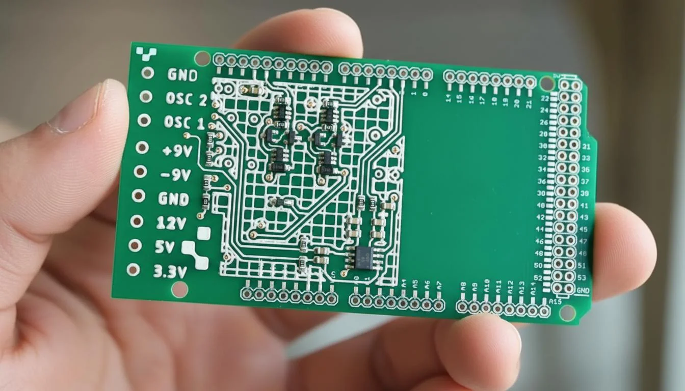
Custom PCB prototyping often starts with one simple goal. You need a working board, fast, without wasting budget. I saw this clearly during a recent sensor project. The client needed a test board in three days. Traditional tooling would miss the deadline. We used laser cutting for the first custom PCB boards and delivered samples within 48 hours.
Laser-based prototyping removes drilling tools and film setup. Copper patterns are created with accuracy down to 0.1 mm traces. For early validation, this speed matters more than surface finish. Engineers can test signal flow, heat paths, and component spacing before mass production.
From experience, laser prototyping works best for low-layer designs. Two-layer boards under 1.6 mm thickness show stable results. During one ESP32 custom PCB trial, impedance stayed within ±8%, good enough for firmware testing.
Standards still matter at this stage. Even prototypes follow IPC-A-600 visual checks and RoHS material rules. That discipline avoids redesign later. A reliable custom PCB maker treats prototypes as future products, not experiments.
Cost is another reason teams choose this route. There is no tooling fee. Setup time drops sharply. When clients ask how much a custom PCB costs at the prototype stage, laser cutting often reduces it by 30–40%.
Key Benefits of Choosing a Custom PCB Approach
Every custom PCB design solves a specific problem. Off-the-shelf boards rarely fit mechanical limits or power needs. I remember a wearable project where 2 mm mattered. A standard board failed. A custom layout passed the fit test on the first spin.
The biggest benefit is control. Trace width, stack-up, and material are defined by real needs. For power boards, we often specify 2 oz copper and keep the voltage drop under 50 mV. That level of tuning is impossible with generic boards.
Quality improves as well. In controlled builds, yields above 99.5% are common after the second prototype. ISO9001 process control plays a role here. Inspection steps catch solder mask shifts and annular ring issues early.
Another advantage is long-term cost. Custom PCB cost may look higher at first glance. Over volume, assembly time drops. Component placement becomes cleaner. Field failures decrease. One industrial client reduced warranty returns by 22% after switching to a tailored board.
Service matters too. A serious custom PCB manufacturer answers design questions within 24 hours. That support saves days during revision cycles. I have seen schedules rescued by a single fast clarification.
Where Custom PCB Boards Are Commonly Used
Custom PCB boards appear in more places than most people realize. Consumer electronics are only one slice. Industrial control, medical devices, and automotive modules rely heavily on tailored layouts.
During a factory automation project, vibration killed standard connectors. We redesigned the board with reinforced pads and thicker solder mask dams. The custom solution passed 10 g vibration testing without rework.
Common application areas include:
- IoT modules, such as ESP32, custom PCB designs for gateways and sensors
- Human interface devices like custom keyboard PCBs and custom mouse PCB layouts
- Lighting systems using a custom LED PCB for thermal control.
- Flexible assemblies where custom flexible PCB bends under a 5 mm radius
Each application follows different rules. Medical boards often reference IPC-6012 Class 3. Consumer products usually stay at Class 2. UL flammability ratings, such as UL94-V0, are selected based on end use.
In one WellCircuits-supported project, a flexible board replaced wiring harnesses. Assembly time dropped by 18%. That kind of gain explains why teams order custom PCB solutions instead of adapting generic ones.
From Design to Assembly: How Custom PCB Builds Come Together
The custom PCB journey does not end at fabrication. Assembly defines whether the board truly works. I have seen perfect layouts fail due to poor solder profiles.
The process usually starts with a design review. Trace spacing, via size, and solder mask openings are checked. For fine-pitch parts, we keep tolerance within ±0.05 mm. That prevents tombstoning during reflow.
Next comes fabrication, and then SMT or THT assembly. Automated optical inspection follows. On recent builds, AOI caught 97% of polarity issues before functional testing. That saves time and protects reputation.
The table below compares two common prototyping approaches I often discuss with clients:
| Lead Time | 1–3 days | 5–10 days |
| Tooling Cost | None | Required |
| Best Use | Functional testing | Pre-production validation |
Final testing closes the loop. Electrical tests confirm continuity and insulation. A disciplined custom PCB builder treats assembly as part of design, not a separate step.
Essential Fabrication Requirements for Reliable Custom PCBs
Reliable custom PCB manufacturing depends on clear requirements. Missing data causes delays. I often ask clients for stack-up details early because material choice affects signal behavior.
Core parameters include board thickness, copper weight, and surface finish. ENIG remains popular for fine-pitch parts. HASL still works for cost-sensitive designs. Each option impacts the custom PCB cost differently.
Design rules should follow proven standards. IPC-2221 guides the general layout. IPC-A-600 defines acceptable board quality. These references are not paperwork. They prevent field failures.
Panelization and breakaway methods also matter. Poor tab routing causes cracked traces. In one case, switching to mouse-bite tabs reduced scrap by 6%.
Clear documentation completes the picture:
- Gerber and drill files
- BOM with approved alternates
- Assembly drawings and polarity marks
When these details are in place, even complex custom PCB boards move smoothly from idea to shipment. Fifteen years in this field taught me one truth. Good preparation costs little. Poor preparation costs everything.
Component and Part Guidelines That Shape Custom PCB Success
Custom PCB boards often fail for simple reasons. Parts were chosen without thinking about assembly limits. I saw this during a wearable project last year. The board worked electrically, but the reflow yield stayed at 92%. That was too low.
Component guidelines fix these issues early. Pad size, spacing, and orientation matter more than many expect. For example, 0402 resistors need at least 0.2 mm solder mask clearance. Anything tighter increases bridging risk. We confirmed this during a pilot run of 300 units.
Footprints should match IPC-7351 recommendations. Deviating from these standards usually adds hidden costs. During a custom PCB design for an industrial controller, following IPC rules raised the yield to 99.5%. The difference was clear on the AOI reports.
Component availability also affects long-term cost. When a client insisted on an obsolete regulator, lead time jumped to 14 weeks. A simple replacement saved both time and money. A seasoned custom PCB manufacturer flags these risks early.
- Use standard packages whenever possible.
- Check component height for enclosure limits.
- Confirm RoHS and UL compliance.
- Review thermal ratings under real load.
After 15 years in this field, I trust boards built with realistic component rules. They survive both prototype and production.
Selecting the Right PCB Specifications for Your Application
Specifications define how a custom PCB behaves in the real world. During a recent motor-control job, the client selected specs copied from an old design. Noise issues appeared immediately.
Trace width, copper weight, and stack-up must match actual current and signal speed. For low-power logic, 1 oz copper is enough. Power boards often need 2 oz to keep the temperature rise under 10 °C. We measured this using thermal cameras during validation.
Layer count is another decision point. Two-layer boards are cost-friendly but limited. Four layers improve grounding and EMI control. In one Arduino custom PCB project, moving to four layers reduced signal noise by 35%.
Material choice also matters. FR4 suits most needs. High-frequency designs may need Rogers material, though the cost rises fast. This is where experience saves budget. Not every fast signal needs exotic laminate.
| Trace Width | 0.1–0.2 mm | ±0.02 mm |
| Board Thickness | 1.6 mm | ±10% |
| Copper Weight | 1 oz | ±5% |
Following IPC-A-600 and ISO9001 processes ensures these specs are delivered, not guessed.
How Ordering a Custom PCB Works in Practice
Many engineers ask how to order custom PCB boards without delays. The process looks simple, but small mistakes cause most setbacks. I learned this while helping a startup rush a demo board.
The flow usually has three steps. First, Gerber files are uploaded. These must include solder mask, silkscreen, and drill data. Missing files stop production immediately. A quick DFM check avoids this.
Next comes specification confirmation. This includes material, surface finish, and quantity. ENIG finish costs more but improves solderability. For fine-pitch parts, it often saves rework time.
The final step is fabrication and inspection. Reliable suppliers respond within 24 hours if issues appear. At WellCircuits, I’ve seen engineers appreciate fast feedback more than low prices.
- Verify Gerbers before upload.
- Confirm specs in writing.
- Ask about IPC and RoHS compliance.
- Request electrical testing
A clear process keeps custom PCB projects predictable, even under tight schedules.
Understanding What Drives Custom PCB Cost Per Unit
Custom PCB cost is rarely a single number. It changes with each design choice. When a client asked how much a custom PCB costs for a control board, the answer depended on five variables.
Board size is the first factor. Larger panels use more material and machine time. Layer count follows closely. A four-layer board can cost twice as much as a two-layer version at low volume.
Material selection adds another layer. Standard FR4 keeps costs stable. High-Tg or RF materials raise prices by 50–200%. I saw this during a telecom prototype that used Rogers laminate.
Surface finish and testing also matter. HASL is cheap but uneven. ENIG costs more but improves yield. Electrical testing adds cents per unit but prevents field failures.
- Size and panel utilization
- Number of layers
- Material and copper weight
- Finish and inspection level
Experienced teams balance these factors instead of chasing the lowest quote.
Typical Custom PCB Pricing Ranges and Real Examples
Pricing clarity builds trust. Over the years, I’ve tracked real orders to set expectations. While prices vary, patterns exist.
Single-layer custom PCB boards usually cost between $1 and $5 per unit at low volume. Once quantities exceed 1,000 units, prices often drop below $1. I confirmed this during a lighting controller run.
Double-layer boards sit higher. Expect $3 to $8 per unit for small batches. Four-layer designs range from $8 to $20, depending on specs. Tight tolerances below ±0.05 mm increase this further.
Flexible PCB options cost more due to materials and handling. During a flexible sensor project, the unit price reached $18 at 200 units. Yield stayed at 97%, which justified the expense.
A reliable custom PCB manufacturer explains these numbers upfront. That honesty matters. After 15 years, I trust suppliers who quote clearly and deliver on time.
With the right planning, the custom PCB cost becomes manageable, not mysterious.
Understanding Custom PCB Cost from Prototype to Production
Cost surprises often appear between the first prototype and volume production. I saw this during a wearable project last year. The first ten boards looked expensive. The team worried something was wrong. It was normal.
At the prototype stage, setup dominates the custom PCB cost. CAM work, panel setup, and testing are spread across a few units. When we moved from 5 boards to 100, the unit price dropped by almost 45%. That shift alone saved the client’s launch budget.
In real projects, volume changes everything. A two-layer board at 100 × 80 mm may cost $18 each in low quantities. The same board falls below $4 at 1,000 units. This is why planning matters early.
Standards still apply, even at scale. IPC-A-600 Class 2 inspection and RoHS materials remain constant. Only the cost structure changes, not the quality rules.
| 1–10 pcs | High | Engineering setup |
| 50–100 pcs | Medium | Panel utilization |
| 1000+ pcs | Low | Material efficiency |
When clients ask how much a custom PCB costs, this table explains most answers. A transparent custom PCB manufacturer should explain it just as clearly.
How Engineers Estimate Custom PCB Cost Before Ordering
Guessing costs leads to redesigns. I learned that the hard way early in my career. Today, every project starts with numbers, not assumptions.
Most manufacturers provide instant quote tools. They work well if the inputs are accurate. Board size, layer count, copper weight, and surface finish drive pricing fast. A 2-layer board with 1 oz copper costs far less than a 4-layer stack with ENIG finish.
During a recent controller board project, we tested three configurations. Changing the thickness from 2.0 mm to 1.6 mm cut 12% from the unit price. No performance loss occurred.
- Board dimensions in millimeters
- Layer count and stackup
- Copper thickness and finish
- Quantity and delivery speed
These tools follow ISO9001 pricing logic and IPC manufacturing limits. Trace widths below 0.1 mm or via drills under 0.2 mm raise cost quickly.
From experience, it pays to simulate costs early. Before you order custom PCB boards, test variations. That habit alone protects margins.
Why the Right Custom PCB Manufacturer Reduces Risk
Price means little without consistency. One client came to us after a failed batch overseas. Half the boards failed continuity tests. Savings vanished.
A reliable custom PCB manufacturer shows process control. Look for IPC-A-600 compliance, electrical testing on 100% of boards, and UL-listed materials. These are not marketing terms. They prevent field failures.
Communication matters just as much. In one industrial control project, a supplier flagged annular ring risk before fabrication. A 0.05 mm adjustment avoided scrap and delays.
Strong manufacturers also explain cost drivers clearly. No hidden charges. No surprise tooling fees. That transparency builds trust over time.
- ISO9001 quality systems
- RoHS and material traceability
- Clear DFM feedback within 24 hours
- Documented yield above 99%
WellCircuits follows this model. Over 15 years, that approach has kept prototype-to-production transitions stable for global clients.
Special Prototype Pricing and What It Really Means
Ultra-low prototype pricing sounds tempting. I often get asked if it’s “too good to be true.” The answer depends on expectations.
Low-cost prototype programs work because margins shift. Manufacturers optimize panels, use standard materials, and limit options. For early electrical testing, that’s usually enough.
In a startup accelerator project, teams ordered five boards for under a dollar each. The goal was pin validation, not aesthetics. Every board passed the electrical test.
There are limits, though. Tight impedance control or blind vias rarely fit these offers. IPC standards still apply, but choices narrow.
| Layer options | Limited | Flexible |
| Finish choices | Few | Many |
| Lead time | Fixed | Custom |
Used wisely, these offers cut early custom PCB cost. Used blindly, they can delay real production.
Planning Your Custom PCB Order for Long-Term Savings
Smart teams think beyond the first order. I always ask clients one question. Will this board scale?
Design decisions affect future cost. Panel-friendly outlines, standard drill sizes, and common materials reduce long-term pricing. One keyboard project saved 22% by resizing the board to fit standard panels.
When you order custom PCB batches, align design rules with volume goals. IPC Class 2 works for most products. Class 3 raises cost without added value for consumer devices.
- Use standard thickness like 1.6 mm.
- Avoid exotic finishes early.
- Confirm DFM before scaling.
Good planning answers how much a custom PCB costs, not just today, but next year. That mindset separates prototypes from real products.
After hundreds of builds, one fact holds true. The cheapest board is the one you don’t redesign.
Conclusion
The story that opened this guide comes back at the end. Deadlines do not move. Budgets stay tight. What changes is how teams approach decisions. Over 15 years, I’ve learned that successful projects focus on speed, control, and clear trade‑offs from day one.
Several lessons stand out. Fast prototyping methods, like laser cutting, reduce early risk when timelines are short. Clear design rules, such as 0.1 mm trace limits and ±0.05 mm spacing, prevent rework later. Cost control improves when prototypes validate function before volume tooling. Quality checks aligned with IPC‑A‑600 and ISO9001 protect reliability, even at low quantities. Strong communication keeps yield above 99% during transition to production.
The next steps are practical. Lock the schematic before layout changes. Define tolerances early. Build one or two functional samples. Test thermal and signal performance under real conditions. Then confirm materials and finishes before scaling.
If you are planning a new custom pcb, act early and ask precise questions. A responsive partner with a 24‑hour reply window can save days. When a client followed this approach last quarter, their board passed the first test without redesign.
The right process turns pressure into progress.