Introduction:
In the era of rapid advancements in portable electronic devices and the increasing popularity of high-density flexible substrates, flexible circuit boards have gained significant traction in IC circuit packaging. This shift has propelled the evolution of flexible substrates towards higher density applications.
Flexible substrates offer notable advantages over rigid counterparts, particularly in ultra-thin chip assembly, flexible electronic system packaging, and medical implantable devices.
Common types of flexible substrates used in IC packaging include BGA (Ball Grid Array), CSP (Chip Scale Package), COF (Chip on Film), and MCM (Multiple Chip Module).
Recently, 3D packaging technology has emerged as a pivotal research area, drawing attention from major semiconductor companies and leading to the availability of practical products.

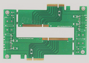
Traditional Manufacturing Engineering of Flexible Substrate:
Traditional manufacturing techniques for flexible substrates encompass methods like the “Roll Reduction Method” and the prevalent “Sheet Metal Processing Method.” Among these, the “Sheet Metal Processing Method” stands out as the most commonly employed approach. The manufacturing flow chart for the double-sided flexible substrate processing method is depicted in Figure 1.
The blanking process for flexible substrates differs from that of rigid ones, requiring blanking of not only the CCL and cover plates but also the cladding and reinforcing panels. During processing, flexible CCL and cladding are rolled, necessitating the use of an automatic blanking machine.
In the drilling process, the fouling removal technique for flexible substrates deviates from that of rigid substrates. To comply with IPC-A-600F standards, the depth of concave corrosion in the fouling removal process must not exceed 50 µm. However, due to polyimide’s vulnerability to strong alkalis, the commonly used potassium permanganate solution for rigid substrates is unsuitable for processing flexible substrates.
Industry typically relies on plasma technology to meet decontamination and concave corrosion depth requirements. Alkaline solutions are generally employed in the PTH process. Prolonged reactions can lead to FPC material swelling, potentially compromising coating adhesion and mechanical properties like ductility. To address this, after the copper layer thickness reaches 0.3 to 0.5 µm during PTH, it progresses to the electroless plating stage until the copper layer attains a thickness of 3 to 4 µm to ensure hole wall integrity for subsequent processing.
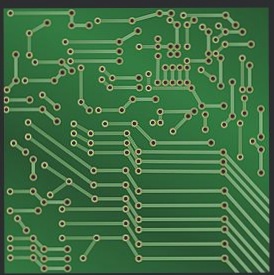
Flexible Substrate Etching Process in PCB Production
- Flexible substrate etching process differs slightly from rigid substrates
- Multiple parallel wires designed at bending sections
- Adjustments to spraying direction, pressure, and solution transmission for etching consistency
After etching, circuit boards undergo treatment to enhance adhesion before overlay alignment. The cladding layer and etched flexible circuit board have varying moisture absorption levels, requiring 24 hours of oven drying before lamination. Stack height should not exceed 25 µm.
Alignment and Lamination of Flexible PCBs
PCBs with cladding layers may use special alignment fixtures or visual magnifying glasses for alignment. Butanone or a hot flame iron aids in positioning post-alignment. Lamination time, heating rates, and pressure selection must align with FPC materials for optimal results. Flexible multilayer substrate lamination complexity surpasses rigid substrates, demanding precise material and processing parameter choices for desired effects. Figure 2 showcases laminated laminate processing.
If you have any inquiries regarding PCB or PCBA, please reach out to us at info@wellcircuits.com.