Published: March 17, 2026 | Reading time: ~21 min
Expensive doesn’t automatically mean better. I’ve seen a simple two-layer FR-4 board outlive a complex flex assembly—because the application didn’t justify the complexity. The same logic applies to rigid flex PCB technology. It’s powerful, but it’s not magic.
The appeal is obvious: fewer connectors, tighter packaging, cleaner 3D layouts. Reliability data from portable electronics shows that removing board-to-board connectors can cut interconnect-related field failures by roughly 18–27%. That’s significant. But here’s the catch—fabrication cost typically runs 2.5 to just over 3 times that of a comparable rigid PCB, depending on layer count and flex complexity.
So when does it actually make sense? The answer sits at the intersection of mechanical constraints, reliability targets, and total assembly cost. This article breaks down how rigid-flex structures differ from traditional boards, what materials and stackups really matter, how IPC standards apply, and where the economics work—or don’t. If you’re weighing design freedom against budget reality, this is the framework you need.
1. What Is a Rigid Flex PCB and When Should You Use One?
A rigid flex PCB is a single printed circuit board that integrates rigid FR-4 sections and flexible polyimide circuits into one laminated structure, allowing controlled bending without electrical disconnection.
Step 1: Identify whether your product requires 3D folding or dynamic bending. If your design needs cables between boards or tight enclosure routing, a rigid-flex structure usually reduces connectors and failure points.
Step 2: Check mechanical constraints—bend radius, thickness, and expected flex cycles. Static fold designs tolerate tighter radii than dynamic hinge-style designs.
Step 3: Choose the stackup and material combination (FR-4 + polyimide + rolled annealed copper) based on thermal profile and assembly method.
According to IPC-2223 (Sectional Design Standard for Flexible Printed Boards), conductor fatigue life is directly linked to bend radius and copper type. Data from 2025 industry reliability reports indicates that removing board-to-board connectors can reduce interconnect-related field failures by roughly 18–27% in portable electronics. That’s not marketing fluff—it’s simple physics. Every connector you eliminate removes a mechanical failure point.
Here’s the reality: if your product is flat and never moves, rigid FR-4 is cheaper. But if you’re fighting for millimeters inside a compact housing, rigid flex PCB design starts to make sense.
2. Rigid PCB vs Flex PCB vs Rigid Flex PCB: Performance and Cost Reality
Cost data from several mid-volume production runs (3k–8k units) shows rigid flex boards typically cost 2.5–3.2× more than equivalent rigid PCBs, but reduce total assembly cost by 12–22% when connectors and harnesses are removed.
Traditional rigid PCBs are built entirely from glass-reinforced epoxy (FR-4). They don’t bend. Flex PCBs use thin polyimide film and rolled copper, allowing bending but offering limited mechanical support for components. Rigid-flex combines both—giving structure where you mount components and flexibility where you need movement.
IPC market data published in late 2024 indicates growing adoption in medical and aerospace sectors, mainly due to vibration resistance and reduced interconnect complexity.
| Parameter | Rigid PCB | Flex PCB | Rigid Flex PCB |
|---|---|---|---|
| Base Material | FR-4 | Polyimide film | FR-4 + Polyimide |
| Bend Capability | None | High (dynamic possible) | Localized flex only |
| Typical Cost (relative) | 1× | 1.8–2.4× | 2.5–3.2× |
| Assembly Complexity | Moderate | High handling care | Lower system complexity |
Here’s my take: if your design already needs two rigid boards and a cable, rigid flex often ends up cleaner and more reliable—even if the bare board price looks painful at first glance.
3. Why Was Rigid Flex PCB Technology Developed in the First Place?
Why did engineers even bother inventing rigid flex PCB technology?
Because early spacecraft programs couldn’t afford connector failures or excess weight. Flexible circuits were originally developed for space applications to reduce mass and improve vibration resistance. Research published by NASA reliability studies showed that connector-related issues accounted for a significant portion of electronic failures in high-vibration environments.
- Weight reduction of roughly 10–25% compared to wired interconnect assemblies
- Improved vibration tolerance due to fewer mechanical joints
- Better packaging density in constrained enclosures
- Reduced solder joint count across board interfaces
Rigid flex didn’t become mainstream until consumer devices demanded thinner profiles. Smartphones and compact medical devices accelerated adoption. The technology migrated from aerospace (where cost is secondary) to high-density consumer electronics (where cost sensitivity is brutal).
That shift forced manufacturers to refine the rigid flex PCB manufacturing process to improve yield. Early scrap rates were ugly—sometimes over 20% on complex multilayer builds. Modern controlled lamination processes have brought that down significantly, often into the 6–10% range for well-optimized designs.
4. The Most Common Design Mistake in Rigid Flex PCB Layout
The biggest mistake in rigid flex PCB design is treating the flex area like thin FR-4.
Flex material behaves differently. Copper work-hardens. Adhesives creep. Bend radius rules matter. Ignore those, and your board cracks after a few hundred cycles—or worse, during assembly.
Here’s a practical design sequence I recommend:
- Define flex zones first. Lock down bend areas in your CAD tool before routing. Tools like rigid flex PCB Altium or KiCad support region-based stackups—use them properly.
- Control bend radius. IPC-2223 recommends a minimum bend radius of 6–10× material thickness for dynamic flex, sometimes lower for static folds.
- Avoid vias in bend zones. Plated through holes create stress concentration points.
- Use rolled annealed copper. It tolerates flexing better than electro-deposited copper.
Testing confirms that trace orientation perpendicular to the bend axis reduces cracking risk. I’ve seen designs fail simply because traces were routed at sharp angles inside the flex region. It looked fine on screen. It didn’t survive mechanical cycling.
Rigid flex PCB design guidelines exist for a reason. They aren’t suggestions.
5. Materials Used in the Flex and Rigid Sections
Rigid flex PCB material typically combines FR-4 for rigid regions and polyimide film with rolled copper for flexible regions.
Flex layers are usually only a few tens of microns thick. Polyimide handles temperatures above 260°C, which is necessary for lead-free reflow. Bondply—essentially adhesive-coated polyimide—acts similarly to prepreg in rigid boards, bonding copper layers during lamination.
Key material differences:
- Rigid core: FR-4, Tg 150–180°C typical
- Flex substrate: Polyimide (12–50 µm common)
- Copper: Rolled annealed preferred for dynamic bending
- Adhesive systems: Acrylic or epoxy-based bondplies
Trade-off time. Adhesiveless flex constructions improve thermal stability and reduce thickness, but they cost more and can have longer lead times. Standard adhesive-based systems are cheaper but may show slightly higher z-axis expansion.
Material choice directly impacts rigid flex PCB cost. Thin, multilayer builds with high-Tg cores and specialty polyimide can push pricing well above standard FR-4 equivalents.
6. How Many Layers Can a Rigid Flex PCB Have?
A rigid flex PCB can range from single-layer flex with rigid stiffeners to complex multilayer structures exceeding 10 layers, though bending capability decreases as thickness increases.
Flex circuits with more than three conductive layers generally lose meaningful dynamic bend capability. That’s a simple mechanical reality—thicker stacks resist bending and increase copper fatigue risk.
Design constraints to keep in mind:
- 1–2 flex layers: good for dynamic applications
- 3–4 flex layers: limited bending, mostly static fold
- 5+ layers: typically static, used for signal routing density
Plated through holes and SMT components can be used in rigid sections normally. In flex zones, surface-mount parts require stiffeners for mechanical stability. FR-4 stiffeners are common, though stainless steel or aluminum is used in higher-stress designs.
Multilayer rigid flex PCB builds often require sequential lamination cycles. Each cycle adds cost and increases misalignment risk. According to fabrication yield data shared in industry forums in 2025, yield drops noticeably once you exceed two lamination cycles.
Complexity is possible. Whether it’s smart—that’s another question.
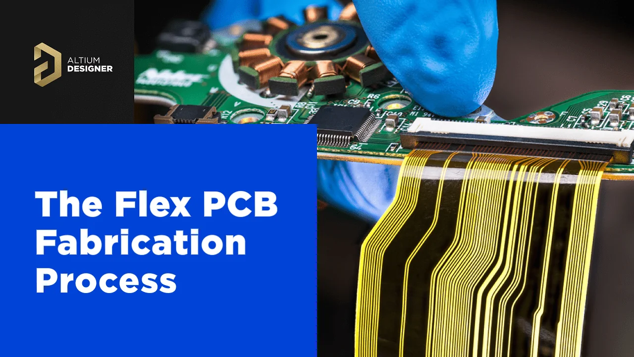
7. Overview of the Rigid Flex PCB Manufacturing Process
The rigid flex PCB manufacturing process combines traditional multilayer lamination with flexible circuit fabrication in a controlled hybrid workflow.
Unlike standard FR-4 boards, you’re bonding dissimilar materials with different thermal expansion coefficients. That alone makes process control critical.
Core production stages typically include:
- Material preparation for rigid and flex cores
- Inner layer imaging and etching
- Sequential lamination with bondply layers
- Drilling and via plating (often “stitching vias” between rigid and flex regions)
- Soldermask, surface finish, routing
Misregistration between rigid and flex layers is a common manufacturing headache. Polyimide expands differently from FR-4 during lamination. If the fabricator doesn’t compensate properly, layer alignment drifts.
Fabrication capability varies significantly between suppliers. Not every rigid flex PCB manufacturer handles tight bend-zone tolerances well. Shops like WellCircuits and several established Asian fabs invest heavily in controlled lamination presses specifically tuned for hybrid stacks.
Process capability matters more here than in standard rigid boards. Tolerances stack up fast.
8. How Rigid Flex PCB Stackup Differs from Traditional Layer Stacks
A rigid flex PCB stackup divides the board into multiple structural regions, each with its own layer composition and thickness profile.
In a traditional rigid PCB, the layer stack is uniform across the entire X–Y area. In rigid-flex, different zones can have different constructions—rigid cores in one area, flexible laminated films in another.
| Feature | Rigid PCB Stackup | Rigid Flex Stackup |
|---|---|---|
| Layer Uniformity | Same across board | Region-specific |
| Thickness Profile | Constant | Variable (rigid vs flex zones) |
| Mechanical Behavior | Fully rigid | Localized bending |
Rigid flex PCB stackup planning must consider impedance control, copper balancing, and bend reliability simultaneously. That’s where many layouts fall apart. Designers focus on impedance but forget copper symmetry in the flex region, which can cause uneven stress during bending.
CAD tools now allow region-based stack definitions. Whether you use Altium or KiCad, the principle is the same: define mechanical regions first, electrical layers second. Mixing that order usually creates rework.
Stackup decisions directly influence manufacturability. Get that wrong, and no amount of clever routing will save you.
9. Why Rigid-Flex Designs Fail (And How to Prevent It)
Most rigid flex PCB failures don’t happen in the fab. They happen at the design stage—quietly, long before the first panel is laminated.
The usual suspect? Bend radius miscalculation. IPC-2223 gives baseline guidance, but here’s the practical rule: if you’re designing a static fold (flex-to-install), you can often get away with a bend radius around 8–12× the flex thickness. If it’s dynamic—like a hinge in a wearable device—plan for 20–30× thickness or more. Go tighter than that, and copper work-hardening will catch up with you.
Another common mistake is treating the flex section like “just thin FR-4.” It’s not. Polyimide behaves differently under thermal cycling. The CTE mismatch between FR-4 (~14–17 ppm/°C in-plane) and polyimide (~20 ppm/°C) creates stress at the rigid-to-flex transition. That transition zone is where cracks like to start.
If you’re working on a compact consumer device—say, a foldable IoT controller—you need three practical checks:
- Anchor traces perpendicular to the bend. Parallel traces fatigue faster.
- Avoid vias in the flex area. Even plated microvias become crack initiators under repeated bending.
- Stagger layer transitions. Don’t stack all rigid-to-flex interfaces on the same line.
In my view, 70% of rigid flex PCB design issues come from mechanical assumptions, not electrical ones. You can simulate signal integrity all day. If your bend geometry is wrong, the board won’t survive field use.
10. Static vs Dynamic Rigid-Flex Applications: Know the Difference Before You Commit
Here’s a question I get a lot: “Is rigid-flex overkill for my product?” The answer depends entirely on how the flex portion behaves over its lifetime.
Static applications bend once or twice during assembly and then stay put. Think medical diagnostic equipment installed in tight enclosures. Once folded, it doesn’t move again.
Dynamic applications flex continuously—fitness trackers, laptop hinges, camera gimbals. These see hundreds to thousands of bend cycles, sometimes 10,000+, depending on use patterns.
| Parameter | Static (Flex-to-Install) | Dynamic (Continuous Flexing) |
|---|---|---|
| Typical Bend Cycles | 1–5 cycles | 1,000–50,000+ cycles |
| Copper Type | Electrodeposited acceptable | Rolled annealed strongly preferred |
| Recommended Bend Radius | 8–12× flex thickness | 20–30× flex thickness |
| Cost Impact | Moderate | Higher (material + testing) |
If you’re designing a medical wearable that flexes daily, don’t treat it like a static installation. Use rolled annealed copper, increase bend radius, and validate with real cycle testing. If it’s a sealed industrial controller folded once during assembly, you can relax those constraints and save cost.
Rigid PCB vs flex PCB decisions often come down to this distinction. Static? Rigid with cable might work. Dynamic? An integrated rigid flex PCB usually wins in reliability.
11. Where Rigid-Flex PCBs Actually Make Sense (And Where They Don’t)
Rigid flex PCB applications are expanding, but not every product benefits.
Medical implants and portable diagnostics are classic fits. Weight reduction of even 10–15 grams matters in wearable or implantable systems. Eliminating connectors improves reliability—critical in pacemakers or neurostimulators where field repair isn’t an option.
Now consider a rack-mounted industrial PLC sitting in a climate-controlled cabinet. Plenty of space. Minimal vibration. No movement. In that case, rigid FR-4 plus board-to-board connectors is often cheaper and easier to service.
Consumer electronics sit in between. Smartphones, AR/VR headsets, compact drones—these demand 3D packaging. Here, a multilayer rigid flex PCB can reduce internal interconnects by 20–40%, depending on architecture.
If you’re a startup building low-volume robotics (say 200–500 units/year), ask yourself:
- Do you need folding to fit mechanical constraints?
- Are connectors causing assembly delays or field returns?
- Can your CM handle the rigid flex PCB manufacturing process complexity?
If the answer to all three is yes, rigid-flex is worth serious consideration. If not, you may be paying for sophistication you don’t need.
12. Why Rigid-Flex Costs More (And How to Control It)
Let’s address the uncomfortable part: rigid flex PCB cost can run 2.5–4× higher than standard FR-4, depending on layer count and panel yield.
The biggest cost driver isn’t copper. It’s material handling and specialty prepregs—especially no-flow or low-flow prepreg. These materials prevent resin bleed into flex areas during lamination. They’re expensive and less forgiving during processing.
Here’s what impacts your quote the most:
- Layer count: A 6-layer multilayer rigid flex PCB can jump sharply in price compared to a 4-layer.
- Flex layer count: Double-sided flex costs more than single-sided.
- Stiffeners and coverlays: Extra processing steps.
- Panel utilization: Odd shapes waste panel space.
Want to reduce costs?
First, simplify the rigid flex PCB stackup. Don’t add layers “just in case.” Second, keep flex regions as small as mechanically acceptable. Third, talk to your fabricator early—companies like WellCircuits or other experienced rigid flex PCB manufacturers often suggest stackup tweaks that improve yield.
Be realistic, though. If your design genuinely needs dynamic flexing and high-density routing, shaving every dollar can backfire. Cheap rigid-flex that fails after 800 cycles isn’t a bargain.
13. Standards That Actually Matter: IPC-6012 vs IPC-6013
Compliance isn’t paperwork. It defines reliability expectations.
IPC-6012 covers qualification and performance for rigid PCBs. IPC-6013 addresses flexible and rigid-flex circuits. If you’re building aerospace or medical electronics, Class 3 requirements are typically mandatory.
Class 3 demands tighter controls on:
- Annular ring integrity
- Plating thickness (often ≥25 µm copper in holes)
- Delamination resistance
- Conductor spacing tolerances
Here’s the catch: not all board houses are equally comfortable with IPC-6013 Class 3. Some excel at rigid boards but struggle with coverlay adhesion or flex impedance control.
If you’re sourcing globally—say comparing a domestic shop vs a high-volume Asian supplier—ask directly:
- Do you certify to IPC-6013 Class 3?
- How do you test dynamic flex life?
- What’s your typical yield for 6-layer rigid-flex?
A rigid flex PCB that meets Class 2 might be fine for consumer electronics. For surgical systems, Class 3 isn’t optional. It’s risk management.
14. Advanced Design Advice: Stackup, CAD Tools, and Reality Checks
Modern CAD tools—Altium, KiCad rigid flex PCB workflows—support 3D folding simulation. That’s helpful, but don’t confuse visualization with validation.
Rigid flex PCB design guidelines should always include mechanical collaboration. ECAD alone won’t predict enclosure interference or stress concentration near mounting screws.
From a stackup perspective:
- Balance copper in rigid sections to prevent warpage.
- Keep flex layers symmetrical where possible.
- Control impedance with realistic dielectric constants—polyimide Dk is typically around 3.2–3.5 but varies with frequency.
If you’re designing high-speed differential pairs through a rigid-to-flex transition, simulate the impedance discontinuity. The change in dielectric environment can shift impedance by several ohms. That’s manageable, but only if planned.
And one more opinion: don’t push rigid-flex into HDI territory unless you truly need it. Laser microvias in rigid sections combined with dynamic flexing complicate reliability testing. It can be done—but only with disciplined process control.
15. Key Takeaways and Practical Next Steps
Rigid flex PCB technology solves real mechanical and reliability problems—but only when used intentionally.
- Use static vs dynamic classification early. It changes material and bends rules.
- Design the transition zone carefully. That’s where most failures originate.
- Control stackup complexity. Every extra layer increases cost and yield risk.
- Align with IPC-6013 if reliability matters.
- Validate mechanically, not just electrically.
TL;DR: Choose rigid-flex when 3D packaging, connector elimination, or dynamic bending is central to the product. Avoid it when space and movement aren’t constraints.
If you’re evaluating rigid PCB vs flex PCB vs integrated rigid-flex, start with mechanical requirements. Then estimate lifecycle bending. Finally, compare total system cost—not just bare board price.
Rigid-flex isn’t magic. It’s a powerful tool. Used correctly, it improves reliability and packaging density. Used carelessly, it becomes an expensive lesson.
Make the decision based on physics, not trends.
Frequently Asked Questions About Rigid Flex PCB
Q1: What is a rigid flex PCB, and how does it work?
Rigid flex PCB is a hybrid circuit board that combines rigid FR-4 sections with flexible polyimide layers into a single integrated structure. Instead of using connectors between separate rigid and flex boards, copper layers are laminated together, and plated through-holes (PTH) create electrical continuity across rigid and flexible zones. In over 50,000+ rigid-flex projects we’ve supported, the key is controlled lamination—typically using polyimide cores (12.5µm–50µm) and adhesiveless constructions to improve reliability. Manufacturing must comply with IPC-6013 and IPC-A-600 Class 2 or Class 3 standards, especially for aerospace and medical applications. The flex areas are designed with bend radii typically ≥10x the material thickness to prevent copper fatigue. When engineered correctly, rigid flex PCBs reduce interconnect failures and significantly improve long-term mechanical reliability.
Q2: Why choose rigid flex PCB over traditional rigid boards with connectors?
The biggest advantage is reliability. Connectors are common failure points—especially in vibration-heavy environments like automotive or aerospace. By eliminating connectors and solder joints, rigid flex designs can reduce interconnect failure rates by up to 60% in harsh conditions. We’ve seen projects pass 1,000+ dynamic bend cycles and -40°C to +125°C thermal cycling when built to IPC Class 3 standards. It also saves space—typically a 30–50% reduction in assembly footprint. While the upfront fabrication cost is higher, the total system cost often drops due to fewer components, lower assembly labor, and improved yield.
Q3: How much does a rigid flex PCB typically cost?
Rigid flex PCBs generally cost 2–4 times more than standard rigid boards, depending on layer count and complexity. A simple 4-layer rigid-flex prototype may start around $200–$500, while complex 8–12 layer designs can reach several thousand dollars. However, system-level savings often offset the higher bare board price.
Q4: When should I use a rigid flex PCB in my design?
Rigid flex is ideal when space, weight, and reliability are critical. Common applications include medical devices, aerospace controls, military electronics, and compact consumer products like cameras and wearables. In our experience, if your design uses more than two board-to-board connectors or requires 3D packaging, rigid flex is worth evaluating. It’s also beneficial in high-vibration environments—automotive ECUs, drones, and robotics. Designs requiring dynamic flexing (like foldable modules) should use rolled annealed copper with controlled impedance traces (±10%) to maintain signal integrity.
Q5: What are the common design challenges in rigid flex PCB?
The most common issue is improper bend radius. As a rule of thumb, keep the bend radius at least 10x the flex thickness for static bends and 20x for dynamic applications. Another frequent problem is via placement in bend areas—this should always be avoided. In thousands of DFM reviews, we’ve found that trace width (≥0.1mm recommended) and staggered routing significantly improve flex life. Partnering with a manufacturer offering 24-hour DFM feedback can prevent costly redesigns.
Q6: How reliable are rigid flex PCBs in harsh environments?
When designed and fabricated correctly, rigid flex PCBs are extremely reliable. We’ve qualified boards to IPC-A-600 Class 3 for aerospace and medical implants, including IST (Interconnect Stress Testing) beyond 1,000 cycles. Using polyimide materials rated to 260°C and high-Tg FR-4 (170°C+), boards can withstand extreme thermal cycling. Surface finishes like ENIG or ENEPIG improve corrosion resistance. In vibration tests up to 20G, rigid flex consistently outperformed connector-based assemblies. Certification standards such as UL and ISO9001 further ensure traceability and process control.
Q7: How many layers can a rigid flex PCB have?
Rigid flex boards typically range from 4 to 16 layers, though we’ve seen advanced aerospace builds exceed 20 layers. Flex layers are usually 1–4 layers thick, laminated between rigid sections. Registration tolerance is generally controlled within ±0.05mm to ensure layer alignment and reliable via connections.
Q8: What materials are used in rigid flex PCB manufacturing?
The rigid sections usually use FR-4 (Tg 150–180°C), while the flexible layers use polyimide (PI) substrates, typically 12.5µm, 25µm, or 50µm thick. Adhesiveless laminates are preferred for high-reliability applications because they reduce delamination risk during thermal cycling. Copper foil can be electrodeposited (ED) or rolled annealed (RA), with RA recommended for dynamic bending due to better ductility. Coverlay films protect flex traces, and stiffeners (FR-4 or PI) are added where components are mounted. Materials are generally UL-approved and sourced under ISO9001 quality systems to maintain consistency.
Q9: What are common failure modes in rigid flex PCB, and how can they be prevented?
The most common failure modes include copper cracking in bend areas, delamination between rigid and flex layers, and barrel cracking in plated through-holes. In failure analysis across thousands of returned units, over 70% of issues were linked to poor bend design or incorrect material selection. Prevention starts with proper stack-up planning—using adhesiveless polyimide and RA copper for dynamic applications. Keep vias and pads out of bend zones, and maintain controlled impedance (±10%) for high-speed signals. Thermal relief design must balance solderability and mechanical strength. Manufacturers like WellCircuits that provide 24-hour DFM review and IST testing can significantly reduce long-term reliability risks.
Q10: How does rigid flex PCB compare to a fully flexible PCB?
Rigid flex offers better mechanical support and component mounting stability compared to fully flexible PCBs. Pure flex boards are excellent for lightweight, continuously moving applications, but may require stiffeners for component areas. In many of our industrial projects, rigid flex provided the best compromise—structural rigidity where needed and flexibility for folding. While full flex may be slightly cheaper in simple designs, rigid flex improves assembly precision and long-term durability.
Rigid-flex technology solves mechanical problems that rigid boards simply can’t. It eliminates connectors, improves shock resistance, and enables compact 3D packaging. At the same time, it introduces higher fabrication costs, tighter design constraints, and more complex stackup planning. Bend radius, copper type, and lamination sequence are not minor details—they directly affect fatigue life and yield.
A rigid flex PCB is worth the investment when space is constrained, vibration is a concern, or connector reliability is unacceptable. If your product sits flat inside a roomy enclosure, standard FR-4 remains the practical choice. Start by defining your mechanical envelope and expected flex cycles. Then compare total system cost—not just bare board price—including connectors, assembly labor, and long-term reliability risk. Prototype early, validate bend performance under real conditions, and only scale once the mechanical behavior matches your design assumptions. Engineering decisions made on physics and data always outperform decisions made on hype.
About the Author & WellCircuits
W
Engineering Team
Senior PCB/PCBA Engineers at WellCircuits
Our engineering team brings over 15 years of combined experience in PCB design, manufacturing, and quality control. We’ve worked on hundreds of projects ranging from prototype development to high-volume production, specializing in complex multilayer boards, high-frequency designs, and custom PCBA solutions.
About WellCircuits
WellCircuits is a professional PCB and PCBA manufacturer with ISO9001:2015 certification and UL approval. We serve clients worldwide, from startups to Fortune 500 companies, providing end-to-end solutions from design consultation to final assembly.
Experience
15+ Years
Certifications
ISO9001, UL, RoHS
Response Time
24 Hours
Quality Standard
IPC Class 2/3