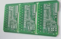
PCB Processing Technology and Assembly Process
Definition:
- PCB Processing Technology involves manufacturing printed circuit boards.
- Assembly Process includes integrating circuit and structural components onto the PCB.
In PCB production technology, manufacturers provide detailed requirements for designers. Focus on manufacturability design for electronic assembly is crucial during the PCB design phase.
Assembly Method and Component Layout
The selection of assembly method and component layout is vital for PCB manufacturability, impacting efficiency, cost, and product quality.
Choosing the Right Assembly Method:
- Recommended assembly methods depend on PCB assembly density.
Understanding PCB Design Manufacturability:
Circuit design engineers must understand the PCB assembly process to avoid common mistakes. Consider assembly density, routing complexity, process flow, and equipment capabilities.
If wave soldering is used, avoid placing SMD components on the soldering surface to prevent complications.
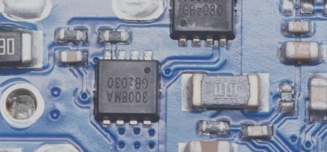
PCB Component Layout
The component layout significantly influences production efficiency and cost, indicating PCB design manufacturability.
- Components should be evenly arranged with consistent orientation and polarity for efficient inspection and soldering processes.
- Only one soldering process can be used on each side of the PCB.
Consider suitable soldering processes for different components. Wave soldering has limitations for SMD components, requiring specific sizes and package types. Proper pin orientation and spacing between components are crucial for wave soldering.
For multi-pin components, add tin-shunting pads to prevent bridging during wave soldering. Align similar component types in the same direction for ease of placement, inspection, and soldering.
Best Practices for PCB Design
Standardizing the orientation of components on a PCB can greatly accelerate insertion and error detection. For instance, ensuring that all radial capacitors’ negative poles face the same side of the board and aligning the notches of dual in-line packages (DIPs) in a consistent direction can streamline the assembly process.
Component Grouping and Alignment
Components of the same type should be grouped together whenever possible, with their first pins aligned in the same direction. This practice enhances organization and ease of troubleshooting during PCB assembly.
Manufacturability Considerations
High assembly densities may necessitate the inclusion of taller components like tantalum capacitors and chip inductors. In such cases, reflow soldering after double-sided solder paste printing becomes essential. Additionally, through-hole components should be strategically placed to accommodate manual soldering, especially in areas where automated soldering processes are not feasible.
Optimizing Soldering Processes
Distributing through-hole components along main straight lines can facilitate selective wave soldering, reducing the reliance on manual soldering and improving efficiency and soldering quality. Concentrated solder joints streamline the soldering process and minimize processing time.
Importance of Positioning Marks
Positioning marks, clamping edges, and process holes are crucial elements in PCB design for automated production. Positioning marks aid optical assembly equipment in accurately aligning the PCB, with diagonal placement and standard shapes enhancing recognition and alignment accuracy.
- Clamping edges of at least 3-5mm width on both the top and bottom of the PCB facilitate automatic transport and prevent assembly issues near the board’s edge.
- Positioning marks, including at least two diagonally placed standard shapes, are essential for optical recognition systems to correct processing errors.
- Positioning marks should be no smaller than their diameter and positioned at least 5mm from the board’s edge for optimal visibility and alignment.
If you have any questions about PCB design, feel free to contact us at info@wellcircuits.com.