Chip-on-Board (COB) Technology: Enhancing PCB Assembly
Introduction to COB
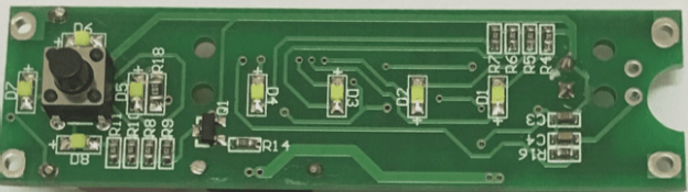
Chip-on-Board (COB) technology involves mounting a semiconductor chip directly onto a printed circuit board (PCB). The chip is connected to the PCB substrate through wire bonding and then covered with resin for reliability. While COB is a cost-effective and space-efficient method, it has some limitations compared to other bonding technologies like Tape Automated Bonding (TAB) and flip-chip bonding.
Benefits and Challenges of COB
- Cost-effective and space-efficient
- Established technology
- Challenges include the need for additional equipment and potential speed limitations
- Strict environmental requirements for PCB assembly
- Potential issues with maintenance
Enhancing IC Signal Performance
Certain COB configurations can improve IC signal performance by reducing parasitic components. However, challenges such as substrate connection issues may arise, impacting performance. It’s essential to address coefficient of thermal expansion (CTE) mismatches and ensure proper substrate connections.
Soldering Methods for COB
Main soldering methods for COB include hot pressure welding, ultrasonic welding, and gold wire welding. Each method offers unique advantages and is commonly used in semiconductor applications.
COB Packaging Process
- Crystal Expansion: LED chip film is stretched using a crystal expander to facilitate handling.
- Adhesive Application: A silver paste layer is applied to the crystal ring, which is then placed on the PCB using a dispenser.
- Chip Placement: LED chip is carefully placed onto the PCB using a piercing pen under a microscope.
- Curing: The assembly undergoes a curing process to ensure stability and reliability.
For more information on PCB fabrication, visit Wellcircuits.
The PCB Manufacturing Process
Step 5: Die Attachment
To ensure proper bonding, a dispenser precisely places red or black adhesive on the designated IC position. Using an anti-static device, the IC die is then carefully placed onto the adhesive.
Step 6: Drying
The attached die is subjected to a constant temperature in a thermal cycle oven on a heating plate for a specific period. Alternatively, natural curing over an extended duration is also an option.
Step 7: Bonding (Wire Bonding)
Utilizing an aluminum wire bonding machine, the IC chip or LED die is connected to the corresponding pad on the PCB using aluminum wire. This establishes the internal lead connections for the COB package.
Step 8: Pre-test
Specialized tools are employed to test the assembled COB board, ensuring it meets specifications. Rework is conducted on any boards that do not pass the test.
Step 9: Dispensing
An appropriate amount of AB glue is applied to the bonded LED die using a glue dispenser. For IC packaging, black glue is utilized. The final appearance is tailored to customer requirements.
Step 10: Curing
The sealed PCB is placed in a thermal cycle oven and kept at a consistent temperature. The curing duration is adjustable based on specific needs.
Step 11: Post-test
Following packaging, the finished PCB boards undergo electrical performance testing using specialized tools to detect any defective units.
If you require PCB manufacturing services, feel free to contact us.