Castellated PCB Guide: Types, Specifications, and Applications for Export-Oriented Businesses

What Are Castellated Holes on a PCB?
With the rapid advancement of high-density electronics, manufacturers increasingly demand miniaturized PCB solutions with enhanced functionality. Traditional through-hole soldering methods often result in cold solder joints due to excessive hole size, compromising electrical connections between motherboards and daughterboards. This has driven global demand for plated half-hole PCB technology – a superior solution for modern board-to-board connections in compact devices.
Castellated Holes (Plated Half-Hole PCB) Explained

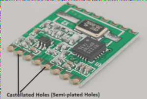
Castellated holes, also called castellations, are semi-plated indentations along PCB edges that enable secure surface-mount assembly of multiple boards. These precision-engineered features:
- Facilitate perfect alignment during PCB module stacking
- Eliminate the need for bulky multi-pin connectors
- Enable direct board-to-board soldering with minimal profile
“Castellated hole technology revolutionizes PCB assembly by combining the reliability of through-hole connections with the space efficiency of SMT components.” – PCB Manufacturing Expert
PCB Manufacturing Process for Castellated Holes
Leading PCB manufacturers in China follow this rigorous process for plated half-hole production:
- Precision drilling of via holes
- Electrolytic copper panel plating
- Image transfer and pattern plating
- Etching and solder mask application
- Surface finishing (ENIG recommended)
- Precision routing to create half-hole profiles
Key Benefits of Castellated Holes for Export Businesses
For international electronics manufacturers, castellated PCBs offer:
- Space-saving solutions for compact device designs
- Simplified assembly of modular PCB components
- Cost-effective alternative to complex connector systems
- Reliable wireless module integration (Wi-Fi/Bluetooth)
Design Considerations for Castellated Holes

When specifying castellated hole PCB designs for export products:
- Minimum diameter: 0.6mm for standard PCBs
- Spacing: ≥0.55mm between holes
- Surface finish: ENIG preferred for reliable soldering
- Pad design: Maximize contact area
Castellated Hole Variants for Different Applications

PCB engineers can choose from multiple castellation types:
- Standard half-holes: Most common for general applications
- Stepped castellations: For connector compatibility
- Microvia castellations: For ultra-high density designs
Industry Applications of Plated Half-Hole Technology

Castellated PCBs are transforming these export-focused industries:
- Telecommunications: 5G modules and base station electronics
- Automotive: Compact ECU designs
- Industrial IoT: Sensor modules and edge devices
- Consumer Electronics: Wearables and smart home devices
Choosing the Right Castellated PCB Manufacturer
When sourcing castellated hole PCBs from China, verify these capabilities:
- Advanced laser drilling equipment
- Strict quality control for plated hole integrity
- Experience with high-frequency PCB materials
- Certifications for export markets (UL, IPC, RoHS)
For export-quality castellated PCBs with competitive lead times, consult with our technical team today.
