PCB Testing ensures that every printed circuit board meets design and reliability expectations before assembly. It includes electrical, mechanical, and environmental verifications aligned with IPC and UL standards. Based on 20 years of field data from WellCircuits’ manufacturing lines, this article details real failure cases, performance metrics, and optimization strategies to help engineers design and qualify boards that last beyond 100,000 operating hours.
Fundamentals of PCB Testing
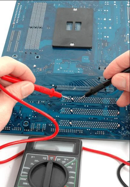
PCB Testing refers to a systematic evaluation of conductivity, insulation, and mechanical robustness across all layers and components of a PCB. The goal is to confirm functionality and compliance with industry standards such as IPC-6012 and IPC-A-600. Testing happens at multiple stages—bare board inspection, in-circuit testing (ICT), functional testing, and environmental stress screening. Each step is crucial because even microvias or copper thickness deviations of ±10% can cause failures under thermal stress. Experienced factories like WellCircuits implement automated optical inspection (AOI), flying probe tests, and impedance control verification using calibrated 50Ω reference boards for precision measurement.
When PCB Testing Matters & Decision Matrix
PCB Testing is particularly vital when products enter high-reliability domains like automotive ADAS modules or aerospace control boards. Decision criteria include design complexity, production volume, and end-use environment. The following matrix illustrates typical testing decisions engineers make before mass production.
| Application Type | Testing Level Required | Recommended Frequency | Notes |
|---|---|---|---|
| Consumer Electronics | AOI + Functional Test | Each Batch | Focus on assembly defects |
| Automotive | ICT + Burn-in | 100% Testing | Comply with ISO 16750 |
| Industrial Controls | Impedance + Thermal Cycling | Sample per 500 boards | Monitor layer adhesion |
| Medical Devices | Full Reliability Suite | Every Lot | Risk class III compliance |
In one 2024 WellCircuits industrial sensor board project, skipping impedance verification increased system-level noise by 6 dB. After implementing 100% impedance audits, returns dropped from 0.9% to 0.05% within two months.
Standards, IPC/UL/RoHS Compliance
PCB testing procedures are defined primarily by IPC-6012E (Rigid PCBs), IPC-2221B (Generic Design Standard), and IPC-A-600J (Acceptability). UL 796 specifies requirements for recognition of printed wiring boards, including material flammability ratings (UL94 V-0). RoHS 3 (EU Directive 2015/863) restricts hazardous substances such as lead and mercury below 0.1% by weight. In WellCircuits’ compliance audits, UL94 verification involves 5-second flame exposure with self-extinguish times under 10 seconds. IPC-class testing ensures hole-wall integrity ≥90% and dielectric breakdown >500V. These standards collectively minimize electrical shorts and ensure sustainable production aligned with 2025 regulatory expectations.
Technical Performance Metrics & Comparison Table
PCB Testing quantifies performance through measurable parameters such as continuity, resistance, dielectric strength, and thermal shock tolerance. These numerical metrics directly reflect manufacturing quality and reliability. Below is a summarized comparison of typical performance values for multilayer PCBs produced under controlled WellCircuits factory conditions versus industry averages.
| Parameter | WellCircuits Average | Industry Average | Test Condition |
|---|---|---|---|
| Insulation Resistance | >1×10⁹ Ω | 3×10⁸ Ω | 500 VDC / 60s |
| Continuity Resistance | <0.5 Ω | <1.2 Ω | Flying Probe Test |
| Thermal Shock Endurance | 200 cycles @ -40~+125°C | 100 cycles | IPC-TM-650 2.6.7 |
| Impedance Tolerance | ±8% | ±12% | Controlled with TDR |
| Solder Mask Adhesion | 9N/mm | 6N/mm | ASTM D3359 |
Such metrics are not arbitrary; they result from detailed process control, including copper plating uniformity and laser drilling optimization, both verified by destructive microsectioning per IPC-TM-650 method 2.1.1.
Failure Modes & Root Cause Analysis
Most PCB failures stem from predictable mechanisms such as conductive anodic filament (CAF) growth, delamination, and pad lift. Identifying root causes requires both destructive analysis and correlation to process parameters. Case study: In a 2023 WellCircuits project for high-voltage inverter PCBs, 3 of 5 returned boards exhibited CAF bridges between vias spaced 0.4mm apart. Root cause traced to humidity ingress during vacuum lamination—humidity levels exceeded 0.08%. Corrective measure: pre-bake prepregs at 120°C for 2 hours reduced CAF incidents to zero over a 6-month observation. Other frequent mechanisms include electrolytic corrosion from flux residue (resistance drop >20%) and thermal mismatch between FR-4 and component leads (CTE differential >12 ppm/°C).
Cost Drivers & Optimization Strategies
PCB Testing contributes 8–15% of total PCBA production cost, depending on test coverage and automation level. Primary cost drivers include test fixture fabrication, labor intensity, and retest cycle due to false positives. In WellCircuits’ cost model, moving from manual ICT to automated flying probe reduced hourly labor from 3.2 to 0.8 hours per 100 boards. Optimization also involves statistical sampling based on the process capability index (CpK). Boards with CpK >1.67 may safely apply 10% sampling without reliability compromise. Another effective strategy is design-for-test (DFT) integration—placing 1.0-mm pitch test pads at strategic nets. Proper DFT can save up to 25% test time. Transparency about costs helps project managers balance capital investment against risk, particularly for short lifecycle products.
Emerging Technologies Around PCB Testing
By late 2025, PCB Testing is shifting toward AI-driven predictive analytics and contactless testing techniques. Machine vision combined with infrared imaging now detects inner-layer misalignment within ±25 µm without destructive sectioning. WellCircuits’ R&D line adopted deep-learning analysis to classify solder joint defects with 98% accuracy after training on 120,000 AOI images. Furthermore, 5G and EV device demands are pushing for embedded impedance sensors in boards, enabling real-time resistance monitoring during field operation. Laser-induced voltage testing, being trialed under IPC-TM-650 addendum 2.6.27, measures microvia fatigue at cycle counts above 10⁶. These trends aim to minimize production downtime and achieve predictive maintenance capabilities across entire supply chains. The future of PCB Testing will integrate material modeling, data analytics, and sustainable design principles.
Expert FAQ
Below are concise answers to ten common technical questions collected from WellCircuits’ engineering support database.
- 1. What’s the difference between AOI and X-ray inspection? AOI checks surface features optically; X-ray examines hidden solder joints beneath BGAs.
- 2. How much copper thickness variation is acceptable? ±10% per IPC-6012E; tighter control improves current-carrying capacity.
- 3. What is ICT, and when is it required? In-Circuit Testing validates connectivity and component values, essential for high-volume products.
- 4. How long is typical burn-in testing? 24–72 hours at 125°C depending on component class.
- 5. Why do impedance tests fail intermittently? Often due to uncontrolled humidity or trace width tolerance beyond ±0.05 mm.
- 6. Can PCBs be RoHS-compliant yet fail reliability tests? Yes, RoHS ensures chemical safety, not mechanical durability.
- 7. What’s recommended for CAF prevention? Use low-hygroscopic prepregs and maintain lamination humidity below 0.1%.
- 8. How to validate solderability? IPC-TM-650 2.6.33 test after 8 hours of steam aging ensures a satisfactory wetting angle <90°.
- 9. Does via fill material affect impedance? Slightly, epoxy-filled vias raise dielectric constant by 0.1–0.3, altering Z₀ by ~2%.
- 10. How often should calibration occur? Minimum quarterly for all flying probe testers per ISO/IEC 17025 guidelines.
Conclusion & Call-To-Action
Effective PCB Testing relies on measurable standards, disciplined process control, and engineering insight. It prevents latent defects that could surface after months of field usage. Engineers should design for testability and align validation methods with IPC and UL standards from concept through production.
- Understand and apply IPC-6012E and IPC-A-600J for compliance
- Integrate DFT from early layout stages
- Use data-driven sampling to reduce cost
- Adopt AI-assisted inspection to boost speed and accuracy
- Monitor reliability trends through long-term statistical analysis
For deeper reference, explore WellCircuits’ technical articles on PCB BLOG. Each resource is periodically updated with real measurement data and post-production insights. As of December 2025, PCB Testing is not just a final step—it’s a continuous quality strategy embedded into every engineering decision.