Understanding Blind and Buried Vias in PCBs
Blind and buried vias are essential components in multi-layer PCBs, particularly those with four or more layers. While traditional vias connect surface layers in two-layer PCBs, blind and buried vias establish connections between inner layers and adjacent surface layers or other internal layers, crucial for high-density PCB designs.
Types of Vias
1. Blind Vias
Blind vias link an inner layer to an adjacent surface layer, visible only on one side of the PCB. These vias, known as “blind,” do not traverse the entire board.
2. Buried Vias
Buried vias connect two internal layers without surface visibility, staying within the PCB stack-up, hence termed “buried” vias.

Advantages and Disadvantages of Blind and Buried Vias
The use of blind and buried vias presents specific benefits and challenges:
- Advantages: Enable higher density designs, reducing the need for extra layers or larger boards, crucial in compact electronic devices with limited space.
- Disadvantages: Manufacturing blind and buried vias increases complexity and cost in PCB production, resulting in higher costs compared to standard multi-layer PCBs.
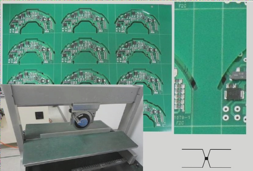
Peck Drilling for Blind Vias
Drilling blind vias accurately is crucial to prevent board damage. Incorrect drill depth can lead to weak connections, rough edges, or board failure. Peck drilling, a method of controlled, shallow cuts in the PCB, helps avoid material buildup and enhance precision.
Wellcircuits employs advanced peck drilling techniques for precise blind vias. This method involves multiple drilling passes to reduce material buildup, preventing air pocket formation and ensuring proper plating for a robust layer connection.
If you have any inquiries regarding PCB or PCBA, contact us at info@wellcircuits.com.