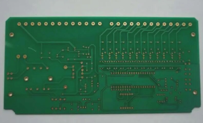
High-Speed PCB Design
The importance of high-speed PCB design is crucial in meeting the growing demand for faster and more complex electronic devices. High-speed PCBs are utilized in various fields like data storage, telecommunications, and high-performance computing.
Power Integrity
Power integrity is essential for ensuring the quality and reliability of a PCB’s power delivery system. At high speeds and frequencies, managing the power supply to minimize noise interference becomes more complex. Maintaining stable voltage references and distributing power while managing noise is crucial for power integrity.
Best Practices for Power Integrity:
- Place decoupling capacitors close to component power pins.
- Keep power traces short and wide with 45-degree or rounded corners.
- Arrange power and ground planes in a stack for optimal performance.
Signal Integrity
Signal integrity focuses on the quality of signals as they travel through the PCB and components. As signal speeds increase, issues like crosstalk, impedance mismatches, and ground bounce can affect signal quality, leading to transmission errors and system failures.
Best Practices for Signal Integrity:
- Use controlled impedance traces to match transmission line impedance.
- Minimize trace lengths to reduce signal degradation and parasitic effects.
Proper Trace Routing Techniques
- Effective trace routing is crucial in PCB design. Key techniques include using vias, avoiding sharp corners, stacking signal layers correctly, and maintaining consistent trace width. Vias are essential for routing but can introduce inductance and capacitance, leading to reflections and impedance changes. It’s advisable to minimize vias in differential traces to prevent issues.
Crosstalk in PCB Design
Crosstalk occurs when electromagnetic interference between traces causes signal distortion. Any conductor carrying a charge generates an electromagnetic field, potentially causing noise and errors. Crosstalk is more pronounced at higher frequencies and speeds, making mitigation strategies vital.
Best Practices to Reduce Crosstalk:
- Position a ground plane near high-speed signal layers to shield and maintain a reference plane, controlling electromagnetic fields.
- Configure adjacent signal layers with crossing routing directions to minimize broadside coupling and reduce crosstalk.
- Avoid placing high-speed signals close to other signals to prevent interference and ensure signal integrity.
Conclusion
Designing high-speed PCBs requires special attention to power and signal integrity challenges. Staying informed about the latest trends and advancements is crucial for both seasoned professionals and newcomers in the field. Continuous learning is key to success.
If you have any inquiries about PCBs or PCBA, don’t hesitate to contact me at info@wellcircuits.com.