Backing Board for PCB Drilling
Phenolic resin laminated boards are commonly used as backing boards for PCB drilling, providing high temperature resistance, deformation resistance, excellent flatness, and suitability for advanced PCB drilling processes. These boards are manufactured through a pressing process to create a laminated, plate-like product. The backing board category is divided into upper covers and lower backing boards, with various material options available for each.
Requirements for the Upper and Lower Plates in PCB Production
- The upper cover plate must meet five essential requirements: flexibility, thickness tolerance, flatness, high-temperature resistance, and low moisture absorption.
- The lower backing plate supports the PCB during processing, protects equipment, and ensures substrate quality. Key requirements include flatness, dimensional tolerance, ease of cutting, a hard and flat surface, and high-temperature resistance.
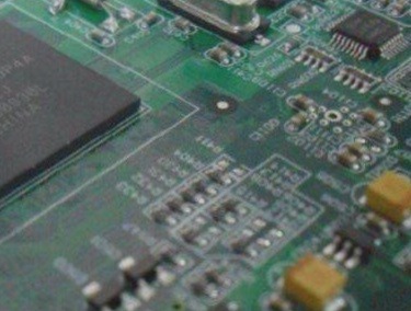
BGA Processing Techniques in PCB Copy Board Technology
Production of Outer Circuit BGA:
Before processing customer data, understanding BGA specifications and design details is crucial. Copper thickness, compensation values, and via-hole spacing are important factors to consider to ensure quality production.
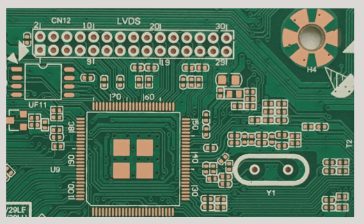
BGA Solder Mask Production
- BGA Surface Mount Solder Mask Opening: The opening range should be between 1.25 mil and 3 mil.
- BGA Corresponding Hole Blocking Layer and Character Layer Processing: Ensure proper plugging and character layer alignment for quality production.
- BGA Plug Hole Template and Backing Layer Processing: Create a 2MM layer for effective PCB circuit layer treatment.
The Plugging Layer (JOB.bga)
To align the 2MM layer with the hole layer, use the *Actions -> Reference Selection* function to reference the 2MM layer. Choose “Touch” for the parameter mode and copy the necessary holes within the BGA’s 2MM range to the plugging layer. Name this layer *JOB.bga*. Note: if the customer specifies that the test hole at the BGA should not be plugged, ensure to select the test hole. A BGA test hole is characterized by having a full window on both sides of the solder mask or a window on one side.
Copying the Plug Hole Layer to the Backing Layer (JOB.sdb)
Lastly, duplicate the plug hole layer onto a separate backing layer named *JOB.sdb*.
Adjusting the Hole Diameters
Modify the hole diameter of the plug hole layer and the backing layer based on the specifications provided in the BGA plug hole file.
If you require PCB manufacturing services, feel free to contact us.