Power PCB Layout and Wiring
In the realm of digital circuits, managing surge current is crucial to prevent high-frequency noise interference with other signals. Parasitic elements like inductance, resistance, and capacitance in high-speed circuitry can exacerbate this issue, reducing the circuit’s ability to handle surge current effectively.
To combat this, adding a bypass capacitor before the digital device is essential. The capacitor’s capacitance must be sufficient to transmit energy within transmission rate limits. Typically, a combination of a large and small capacitor is employed to cover the full frequency range.

Avoiding Hot Spot Generation
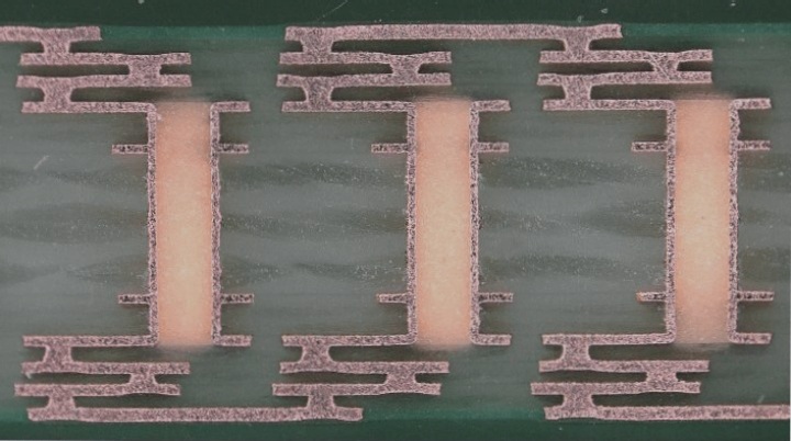
During through-hole placement, vigilance is required to prevent hot spot generation. Signal through-holes can create voids in power layers, leading to increased current density in specific areas, known as hot spots. To mitigate this and potential EMC issues, through-hole placement should incorporate a mesh pattern to ensure uniform current density and prevent isolation of the plane.
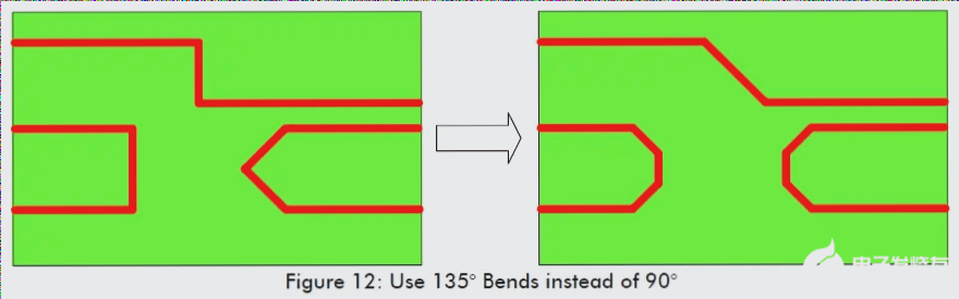
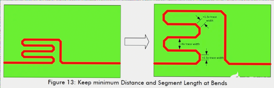
Bending Mode of PCB Routing
When routing high-speed signal lines, minimizing bending is key. Sharp angles should be avoided in favor of obtuse angles, and snake lines can help maintain consistent length. Careful consideration of line width, spacing, and bending mode is crucial, with adherence to the 4W/1.5W rule.
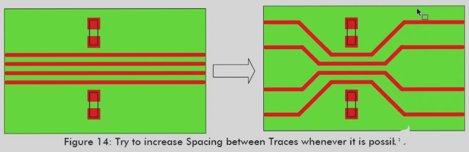
The Proximity of Signal Lines
Closely spaced high-speed signal lines can lead to crosstalk issues. Increasing separation between these lines near bottlenecks is recommended to mitigate crosstalk problems and maintain signal integrity.
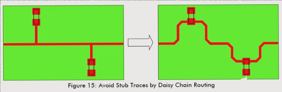
PCB Routing Stubs
Long stub lines can act as antennas, potentially causing EMC problems and signal reflections. Proper management of stub lines, especially those longer than 1/10 of a wavelength, is crucial to prevent these issues.
Impedance Discontinuity
Impedance values of traces are influenced by line width and distance from the reference plane. Addressing impedance discontinuity, especially between interface terminals and device pads, is vital to prevent signal reflection. Proper layout strategies like using copper sheets can help ensure impedance continuity.
Impedance Discontinuity in PCB Design
- Perforations can cause impedance discontinuity in PCBs.
- To minimize this effect, remove unwanted copper sheeting for inner and through connections during the design phase using CAD tools or by contacting PCB manufacturers.
Optimizing High-Speed Differential Signal Lines
- Ensure equal width and spacing for high-speed differential signal lines to achieve specific impedance values.
- Avoid placing holes or components in the lines to prevent EMC issues and impedance discontinuity.
Symmetrical Arrangement for Differential Signal Lines
- High-speed differential signal lines may require serial coupling capacitors arranged symmetrically with recommended package sizes.
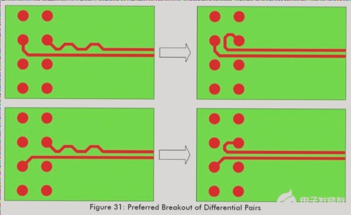
- Minimize through-holes for high-speed pairs, and if necessary, arrange them symmetrically to avoid impedance discontinuity.
Considerations for Isometric Problems
- Ensure arrival time and delay error considerations for high-speed signal interfaces like buses.
- Use serpentine lines to achieve equal length for strict time delay requirements in differential signal lines.
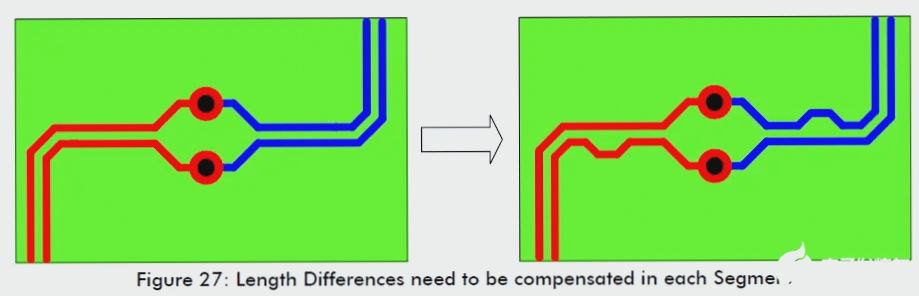
Equal Length Processing in PCB Wiring
- Wiring bending contributes to length loss in PCBs.
- Keep the length between bends close (<=15mm) to achieve equal length processing.
Equal Length for High-Speed Differential Signal Lines
- Ensure independence and equal length for different parts of high-speed differential signal lines, including through-holes, series-coupling capacitance, and interface terminals.
LVDS Display Devices and PCB Expert Tips
For interfaces like LVDS display devices, precise timing sequence requirements and minimal time delay are crucial for differential signals. Compensation within the same plane is necessary due to varying signal speeds at different layers.
Expert Advice:
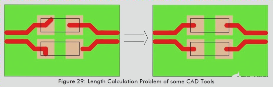
- Some EDA software calculates wiring length including the pad interior, affecting accuracy. Be cautious when using such software.
- Opt for symmetrical routing to avoid serpentine paths for equal length whenever possible.
Additional Tips:
- Consider adding a small loop at the short differential line’s source for compensation if space allows, instead of using a serpentine line.
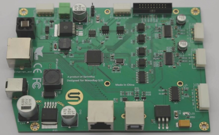
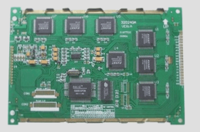
Understanding PCBs
- PCB, or printed circuit board, is a vital component in modern electronics.
- It offers a stable base for electronic components to connect and communicate effectively.
- PCBs are composed of non-conductive materials like fiberglass with copper foil layers for signal pathways.
- The PCB creation process involves layout design, circuit printing, and copper layer etching.
- Electronic components are soldered onto the PCB to form functional circuits.
- PCBs vary from single-sided to multi-layered boards, catering to different needs.
- Advancements in PCB tech enable smaller, more efficient circuits for powerful electronic devices.
- Staying updated on PCB tech and manufacturing is crucial for producing high-quality boards.