Decoding Multi-Layer PCB Structures: A 3D Visualization Guide for Electronics Manufacturers
In today’s competitive global electronics market, understanding multi-layer PCB architecture is crucial for hardware engineers and PCB sourcing professionals. This comprehensive analysis reveals how advanced 3D modeling helps visualize complex board structures that power modern electronics.

Why Multi-Layer PCB Analysis Matters for Export Businesses
As demand grows for high-performance electronics manufacturing in China, international buyers need to understand:
- Cost-performance ratios of different PCB configurations
- How to choose between through-hole vs. HDI boards for specific applications
- The best PCB stackup for various product categories
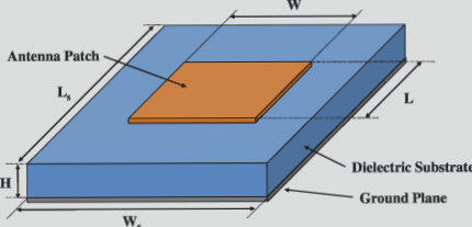
Core Components of Multi-Layer PCB Architecture
The foundation of high-quality PCB manufacturing lies in three key elements:

“Understanding PCB layer structures separates successful hardware projects from costly failures in international electronics trade.”
PCB Type Breakdown for Global Buyers
1. Through-Hole Technology (Standard Multi-Layer)
- Best for: Cost-sensitive projects requiring reliable interconnects
- Typical applications: Industrial controls, automotive electronics
- China manufacturer tip: 0.2mm holes increase cost by 15-20%

2. HDI Boards (High-Density Interconnect)
- Best for: Compact consumer electronics like smartphones
- Key advantage: Enables 30-50% size reduction vs. conventional PCBs
- Export consideration: Laser drilling increases unit cost but reduces assembly expenses
Layer Count Strategies for Different Applications
| Product Category | Recommended Layers | Cost Factor |
|---|---|---|
| Basic Microcontrollers | 2-layer | Most economical |
| IoT Devices | 4-6 layer | Balanced performance |
| Smartphone Mainboards | 8-10 layer HDI | Premium solution |

Advanced PCB Technologies for Export Markets
Laser Microvia Technology
Modern Chinese PCB factories now offer:
- 50μm laser holes for ultra-HDI designs
- Staggered via configurations for high-speed signals
- Any-layer interconnect solutions (premium option)
Material Innovations
Leading PCB suppliers in Shenzhen are adopting:
- Low-loss dielectrics for 5G applications
- High-Tg materials for automotive electronics
- Flex-rigid combinations for wearables
Cost-Saving Strategies for International Buyers
When sourcing multi-layer PCBs from China, consider:
- Standardizing hole sizes across designs
- Consolidating orders for volume discounts
- Working with certified PCB manufacturers to reduce defect rates
Future Trends in PCB Export Markets
The global PCB industry is evolving with:
- Growing demand for automotive-grade PCBs
- Increased adoption of embedded component technology
- Shift towards sustainable PCB manufacturing processes
Key Questions International Buyers Should Ask
- How does layer count affect my product’s EMI performance?
- What are the lead time differences between 4-layer and 6-layer boards?
- Which Chinese PCB factories specialize in high-mix, low-volume production?
Understanding these multi-layer PCB fundamentals helps global buyers make informed decisions when sourcing from China’s electronics manufacturing hubs.