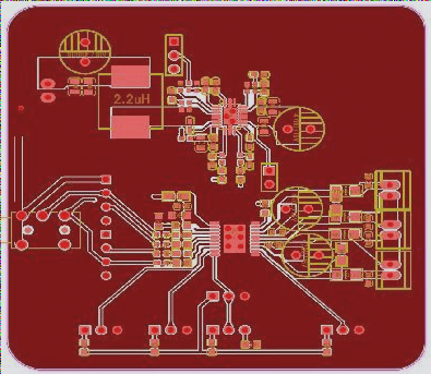
Bridging in PCBs
Bridging in PCBs is a common issue that can occur due to various factors such as excessive solder, edge collapse after solder printing, PCB substrate solder area being out of tolerance, and SMD placement offset. As circuits continue to miniaturize, bridging can lead to electrical short circuits, affecting the product’s functionality.
Poor Wetting in Soldering
Poor wetting is a phenomenon where the solder and PCB substrate fail to create a metal-to-metal reaction during soldering, resulting in insufficient or unsuccessful solder joints. Contamination on the soldering area’s surface, solder resist, or the presence of a metal compound layer on the joined object’s surface can cause poor wetting.
Factors like sulfides on silver surfaces, oxides on tin surfaces, or excess residual aluminum, zinc, cadmium in the solder can lead to poor wetting. Gas on the PCB substrate’s surface, especially in wave soldering processes, can also contribute to this issue.
To prevent poor wetting, it is crucial to follow proper soldering procedures, implement anti-fouling measures on PCB substrate and component surfaces, select the right solder, and establish suitable soldering temperatures and times.


