Understanding System-Level Synchronous Switching Noise (SSN) in FPGAs
Modern CMOS technology allows FPGAs to feature multiple I/O interfaces, emphasizing low power consumption for high-speed interfaces. Decreasing voltage to save power can, however, reduce the noise margin allowed by I/O interfaces. Accurate measurement and quantification of system-level SSN across chips, packages, and PCBs are essential for FPGA users.
SSN Analysis and PCB Board Design Techniques
SSN, particularly synchronous switching output noise (SSO) from FPGA output buffering, differs from input buffering-induced SSN. This article explores the factors contributing to system-level SSO, suggesting a hierarchical modeling approach. Learn how to align the SSO model with frequency and time domain measurements and discover effective PCB design techniques to mitigate SSO.
The Formation of System-Level SSO
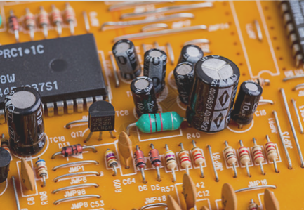
A PCB with an FPGA comprises wafer, package, and board sections. Quantifying SSO at PCB trace ends connected to FPGAs is crucial due to power distribution network impedance and mutual inductive coupling between switch I/Os. The PDN, spanning wafer, package, and board components, powers CMOS circuits. Rapid current changes induce voltage fluctuations, while mutual inductive coupling around chip edges generates transient I/O currents and voltage noise.
Modeling System-Level SSO
A layered model predicts SSO on PCBs, incorporating output buffer, PDN, and signal coupling models. The interaction between these models bridges the chip package and PCB board levels, considering power/ground planes, capacitors, vias, and signal traces. This hierarchical modeling approach balances accuracy and computational efficiency for complex systems.
Design Methods to Reduce SSO
For PCBs with FPGAs, two fundamental design strategies based on SSO generation mechanisms are outlined, aiming to mitigate noise and enhance signal quality.
Design Methods to Reduce Inductive Coupling
- The simulation results indicate that inductive coupling at the chip package/PCB interface leads to high frequency spikes in the SSO waveform.
- To minimize inductive coupling, attention should be given to utilizing thinner PCB boards and routing key I/Os on shallower signal layers.
- Shortening the distance between I/O vias and ground vias can also help reduce crosstalk.
- Special connections between I/O pads and ground/VCCIO planes have shown a reduction in ground bounce and power sag.
- Experimental tests demonstrated a 17% reduction in ground bounce on AF30 in Bank 1 compared to G30 in Bank 2, with a 13% decrease in power sag.
- Programmable ground pins can aid in reducing SSO by shortening the distance between disturbing and disturbed loops.
Reducing PDN Impedance through Effective Design
- The impedance between VCCIO and ground pins on the PCB interface is crucial for evaluating the PDN performance of an FPGA chip.
- Employing decoupling strategies and using thinner power/ground plane pairs can help reduce input impedance.
- Shortening the length of power vias connecting VCCIO solder balls to the VCCIO plane is an effective method to lower impedance.
- Arranging the VCCIO plane closer to the top layer of the PCB can further reduce impedance.
Latest Insights:
Recent research has shown that incorporating advanced signal integrity analysis tools can greatly assist in identifying and mitigating inductive coupling issues in PCB designs. By leveraging these tools, designers can gain deeper insights into signal loop characteristics and optimize routing strategies to minimize electromagnetic interference.