EMI Problem Solving Techniques for PCB Design
- Using EMI suppression coatings
- Selecting appropriate EMI suppression parts
- EMI simulation design
Controlling EMI Radiation with PCB Layer Stacking
Proper PCB layer stacking plays a crucial role in controlling EMI radiation. Here are some design techniques:
Power Bus Optimization
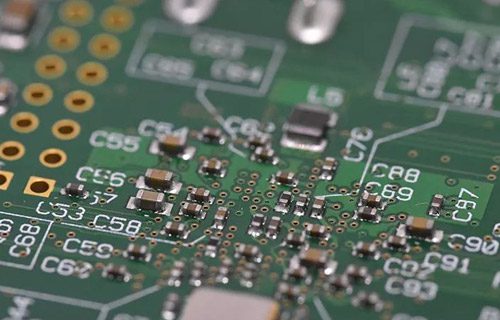
Placing capacitors near IC power pins improves voltage stability. However, addressing harmonic power and transient voltages is essential to reduce common-mode EMI interference. Designing a low-inductance power layer surrounding the IC can help capture excess energy and support a clean output.
Advanced PCB Layer Stacking Strategies
- For circuits with rise times of 100 to 300 ps, consider layer spacing of less than 1 mil and high dielectric constant materials like ceramics.
- For common circuits with 1 to 3 ns rise times, 3 to 6 mil layer spacing and FR4 materials are sufficient to manage harmonics and minimize transient signals.
- Electromagnetic Shielding: Optimal layering places signal traces adjacent to power or ground layers to reduce EMI.
Optimizing PCB Stacking
Layering power and ground layers effectively can aid in shielding and EMI suppression. Consider a stacking scheme where power supply current flows on a single layer with multiple voltages distributed across different parts.
Challenges of 4-Layer Board Design
Traditional 4-layer boards may face challenges due to large distances between power and ground layers. Exploring alternative layering strategies is crucial for effective EMI management.
Cost-effective 4-Layer PCB Design Options
If you are looking to minimize costs, you may want to explore these two conventional 4-layer PCB alternatives. While both options can improve EMI suppression, they are best suited for applications with low component density and ample space around components.
1. Ground-Signal/Power-Signal Layer Arrangement
This design involves having the outer layers of the PCB dedicated to ground, with the inner two layers serving as signal/power layers. By routing the power supply on the signal layer using wide lines, you can reduce path impedance for the power supply current and decrease the impedance of the signal microstrip path. This configuration is highly effective for EMI control.
2. Power-Ground/Signal-Signal Layer Configuration
In this setup, the outer layers carry power and ground while the inner layers handle signals. While this design offers some improvement over the traditional 4-layer board, the interlayer impedance remains similar. Careful arrangement of traces beneath the power and ground copper islands is crucial to control trace impedance. It is also essential to interconnect copper islands on the power supply or ground layers extensively to ensure proper DC and low-frequency connectivity.