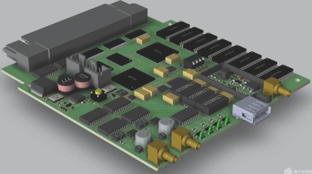
USB Interface Evolution and PCB Design Guidelines
USB, short for Universal Serial Bus, serves as a standardized interface for connecting computers and external devices. It simplifies the connection process and is widely favored for its compatibility, cost-effectiveness, and user-friendly nature.
USB has evolved through various versions like USB 1.0, 2.0, 3.0, and 4.0, with different types (A, B, C, Mini) catering to specific device designs.
Layout Guidelines for PCB with USB Interface
- Position the USB interface near the PCB edge for easy access. Include ESD protection and common-mode inductors for optimal performance.
- Ensure proper distance between ESD components and the USB interface for post-soldering considerations.
Routing Guidelines for USB Interface on PCB
- Maintain a 90-ohm impedance for USB differential pairs, limiting trace length to 1800 mils.
- Minimize trace length and via usage for high-speed signals to maintain impedance control.
- Use return ground vias with signal vias for impedance continuity when changing layers.
PCB Design for USB Type C Interface
USB Type C offers a slim design and faster data transfer, with a reversible plug for easy insertion. The pinout diagram below illustrates the USB Type C interface for modern devices.
Equal-Length Differential Pairs and USB Versions Comparison
USB Type C Plug Pinout
Latest PCB Design Guidelines for Type C Interface:
- Ensure ESD protection, common-mode inductors, and capacitors are positioned near the Type C interface in the sequence: ESD -> Common Mode Inductor -> Capacitor. Maintain adequate spacing between ESD protection and the Type C interface, considering post-soldering conditions.
- Position coupling capacitors for TX signal lines close to the interface, while coupling capacitors for RX signal lines are placed at the device end, as indicated in the diagram below.
Important Type C Trace Design Considerations:
- Keep a differential impedance of 90 ohms ±10% for Type C traces. Ensure the reference plane is solid without splits for impedance consistency, and limit the number of vias when moving across layers to two.
- Route the four sets of differential signals for Type C adjacent to at least one ground plane, with a maximum trace length of 6000 mils. Maintain matched lengths for Type C differential pairs with a maximum mismatch of less than 6 mils.
- Prevent interference with adjacent traces by maintaining a distance of at least four times the trace width between Type C differential pairs and other signals.
- Emphasize the importance of CC1/CC2 pins for connection detection and orientation determination by appropriately thickening the traces during PCB routing.
Additional Information:
- For Type-C connectors operating at speeds ≥8Gbps, adhere to specific design requirements for high-speed signal integrity.
- When routing within the connector, ensure traces exit from the center and add a GND via adjacent to high-speed signals lacking a nearby GND pin.
- For interfaces operating at ≥8Gbps, utilize connectors compliant with relevant standards (e.g., HDMI 2.1, DP 1.4, PCI-E 3.0) from reputable manufacturers like Molex, Amphenol, HRS, etc.
- Depending on the interface chosen, excavate one or two ground layers accordingly beneath the connector pads and designate separate reference planes if needed.
- Place two ground vias near each ground pad for the connector, ensuring close proximity for optimal grounding.