Advanced HDI PCB Production and Multilayer PCB Setup for Cutting-Edge Technological Solutions
Advanced model PCB designs form the core of cutting-edge digital solutions needed to keep pace with the rapidly advancing global technology landscape. Advanced digital requirements demand innovative solutions which multilayer Printed Circuit Boards (PCBs) and High-Density Interconnect (HDI) PCBs fulfill through their provision of portable, reliable high-speed services for numerous applications. This site examines the processes and value of multilayer PCB assembly and HDI PCB manufacturing as well as the necessary PCB fabrication procedures including choice and area strategies.
What Are Multilayer PCB Assembly Setting Up?
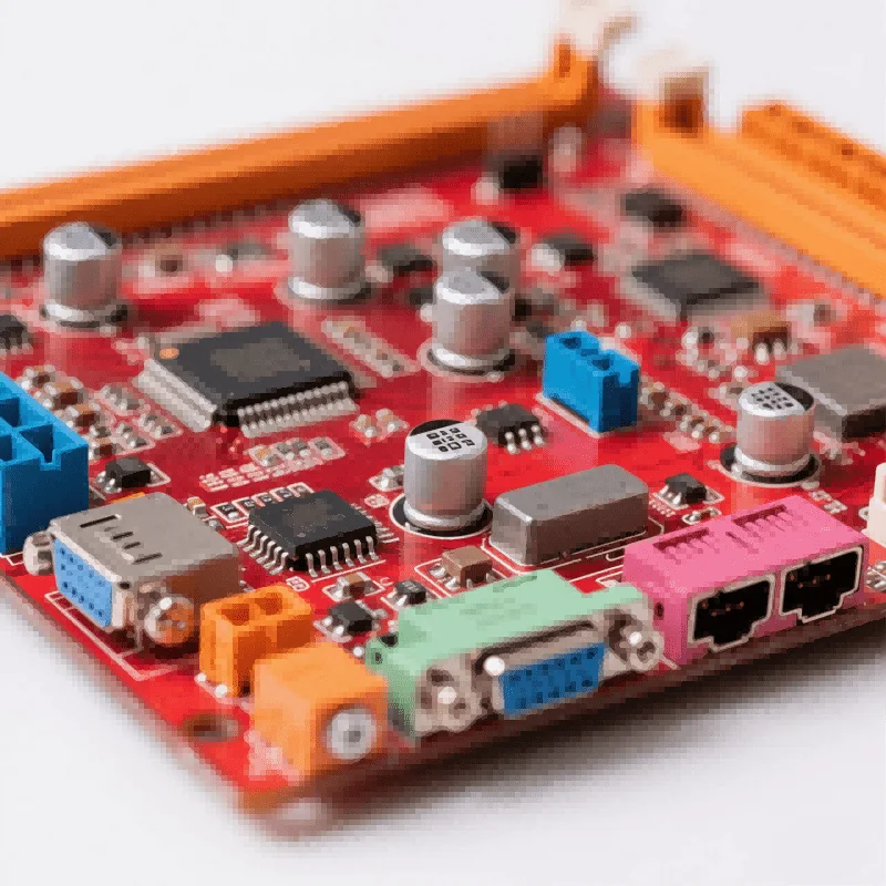
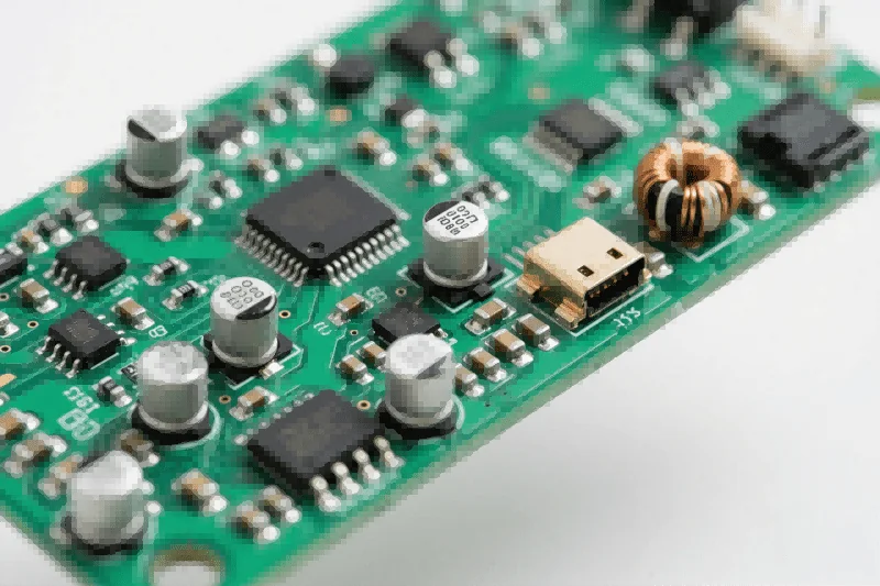
Multilayer PCBs feature three or more conductive layers stacked together and separated by insulating materials necessary for printed circuit board assembly in mass production and custom runs. Multilayer boards deliver increased circuit thickness and functionality inside a compact design which enables easy PCB setup for different applications unlike single or double-sided PCBs. For low-volume production scenarios where high-speed circuits and consistent quality are essential, these PCBs provide vital support to necessary tools.
The key capabilities of multilayer PCBs facilitate advanced applications and efficient PCB assembly processes which turns PCB assembly into an easy fact.
The small physical footprint of HDI PCBs makes them essential for modern electronic devices as they maximize space efficiency.Multiple layers reduce the board’s total size making it perfect for small tools and portable devices while also making the PCB design process more cost-effective.
High PerformanceEnhanced functionality meets advanced computer and communication requirements while advancing next-generation PCBA services through innovative design methods and extensive industry experience.
Layer piling helps reduce electro-magnetic disturbance (EMI) while boosting signal quality to achieve trusted performance in high-performance PCB prototypes.
What Are HDI PCBs?
HDI PCBs advance PCB design by integrating complex features like microvias and specialized digital parts.
The production of HDI PCBs depends on microvias because they enable denser circuit layouts and improved performance during mass PCB assembly which results in a dramatic reduction of the needed space. : The tiny vias enable connectivity between different layers.
Multilayer PCBs depend on blind and hidden vias which connect specific layers without passing through the board for performance enhancement.
Thin and lightweight construction makes modern high-tech devices more efficient when they require both through-hole and surface mount technologies.
Modern digital tools need high component density especially for low-volume manufacturing runs because maintaining high quality becomes essential.
HDI PCBs represent an evolutionary step forward from multilayer PCBs because they meet the requirements of high-speed interactions and high-frequency efficiency while supporting compact electronics within volume PCB manufacturing contexts.
The Significance of Multilayer and HDI PCBs.
Sectors which require precise functionality alongside compact design depend on multilayer and HDI PCBs for efficient performance. Printed motherboard setup performance improves while reliability increases when sourcing parts through single vendor solutions.
Through space optimization, Room Efficiency Multilayer and HDI PCBs enable designers to fit additional components into reduced area sizes. Mobile devices including smartphones and tablets together with wearable technology require essential PCB layout and design for economical production.
Advanced construction methods for PCBs enable the creation of more detailed designs and efficient assembly of larger quantities during low-volume production runs. These PCBs excel in complex circuit support making them perfect for advanced applications like IoT devices and AI technologies which demand extensive BOM documentation.
The fabrication of PCBs requires reliable construction and durable materials to guarantee consistent production efficiency. Innovative manufacturing techniques create durable PCBs that withstand extreme environmental conditions making them suitable for aerospace, automotive, and clinical uses while setting up model PCBs.
The performance of electronic devices benefits from better PCB manufacturing efficiency. Multilayer and HDI PCBs become critical components for high-speed and high-frequency applications in modern digital elements because they offer reduced EMI alongside high signal integrity and low power consumption during PCB setup procedures.
What Are HDI PCBs?
The complete PCB Assembly Manufacturing Process moves an idea into a tangible product.
The construction of multilayer PCBs and HDI PCB manufacturing demands exact planning and execution during box construct setup to enhance both lead time and operational efficiency.
Here’s a detailed introduction:
Both Design and Prototyping stages play a vital role in producing PCBA solutions which ensure quality outcomes for each delivery. PCB prototype creation starts by developing detailed CAD designs necessary for both successful prototype development and efficient assembly pick and place operations. Minimum manufacturing specifications are achieved through decisions regarding layer count and product selection as well as material usage types. Prototyping enables engineers to validate and test circuits before moving into automated production.
Preparing materials ensures the assembly line has access to the appropriate amount of necessary materials. Applications determine the selection of premium substratums, copper foils, and prepregs which serve as protecting layers. FR-4 materials along with polyimide and Rogers laminates find common use in small scale assembly line production.
The process of layer stacking and lamination combines conductive and protective layers through heating and stress application which is essential for producing quality multilayer PCBs and achieving ideal production lead times. HDI PCBs utilize advanced techniques such as consecutive lamination to create microvias and blind/buried vias.
Reliable electrical connections in PCB construction depend on the critical processes of Exploration and Via Development. Precision drilling machines create via holes which then receive conductive material layers to establish electrical connections during PCB construction procedures to maintain superior PCBA quality. Precision laser drilling techniques enable the creation of microvias within HDI PCBs essential for the efficient installation of complex components such as BGA and QFN.
During PCB production both etching and pattern marking are crucial procedures that determine circuit layout and therefore influence the overall performance of the printed circuit board assembly. The chemical etching process eliminates excess copper while preserving the intended circuit layout in the PCB blueprint. New etching technologies enable HDI PCBs to reach precise line widths and spacing suitable for BGA and QFN packages.
Correct component placement is essential for populating the PCB with difficult-to-obtain digital components. Surface Mount Technology (SMT) enables the construction of elements onto the PCB which improves setup performance and results in quicker preparation times. Automated pick-and-place machines deliver precise results whereas reflow soldering in a reflow oven creates reliable connections required for cost-effective PCB setup.
The PCB construction process requires Evaluation and Testing to ensure electronic components meet continuous high quality standards. The combination of Automated Optical Examination (AOI), X-ray assessment and useful screening makes sure that PCBs meet high quality standards and performance criteria before they are shipped.
“Unlocking Advanced Electronics: “Unlocking Advanced Electronics: The Uses of High-Density and Multilayer Printed Circuit Boards” explains how advanced PCB designs benefit industrial applications.
The essential nature of various industries stems from the powerful performance and adaptability of multilayer and HDI PCBs.
Advanced printed circuit card (PCB) layouts and setup solutions drive the following markets.
The consumer electronic market demands advanced printed circuit boards for smart devices alongside laptops and pc gaming consoles as well as wearable technology.
The Automotive field which incorporates Advanced Vehicle driver Aid Equipment along with in-car home entertainment systems and electrical car components requires highly precise PCB designs to manage significant production volumes.
Specialized printed circuit boards (PCBs) serve as essential components for clinical instruments including imaging systems and mobile wellness surveillance devices to achieve maximum performance.
High-grade PCB models support the Aerospace and Defense sectors with their intricate digital systems which require large testing quantities. Applications that utilize high-performance PCB assembly solutions include navigation systems and interaction equipment alongside avionics.
The Telecoms sector through its components such as 5G infrastructure and high-speed routers alongside satellite communication devices demonstrates essential support for advancing PCB assembly services.
Selecting the ideal production partner
Establishing a partnership with a trustworthy PCB manufacturer plays a crucial role in achieving the best results. The following elements should be examined to understand how centroid doccuments affect manufacturing performance.
Quality electronic solutions require both experience and knowledge in prototype PCB setup.
PCB manufacturing technological capabilities enable manufacturers to produce prototype volumes necessary for digital tool production while they must implement state-of-the-art equipment like silkscreen printing to follow standard industry practices in their PCB assembly services.
The quality standards of PCB assembly services need to guarantee both reliability and functionality.
An ideal partner provides support through layout assistance as well as prototyping and comprehensive assembly solutions.
Conclusion
The newest advancements in modern technology consist of manufacturing complex motherboards that have multiple layers and High-Density Interconnect features which enable the production of cutting edge electronic solutions and simplified quick-turn PCB assembly. Companies can create small efficient space-efficient tools that meet today’s open market needs by applying advanced PCB strategies while producing small quantities.
Both next-generation consumer electronics and essential medical devices need multilayer and HDI PCBs to provide the precision and reliability you demand. Work with a trusted PCB manufacturer like WellCircuits to transform your innovative designs into reality while maintaining your competitive edge in the rapidly changing electronics market through quick delivery times.