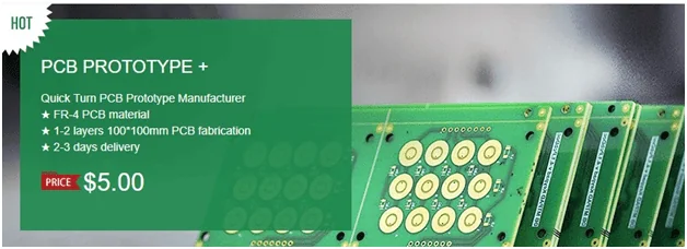
The Complete Guide to PCB Prototyping: Design Workflow and Manufacturing Process
In today’s competitive electronics manufacturing landscape, understanding the PCB prototyping process is critical for businesses looking to develop reliable circuit boards efficiently. This comprehensive guide explores the essential stages of printed circuit board development, offering practical insights for international electronics manufacturers and OEM procurement specialists.
Why PCB Prototyping Matters in Modern Electronics Manufacturing
Before diving into mass production, PCB prototype development serves as the crucial testing ground for design concepts. As a leading PCB manufacturer in China, we’ve identified prototyping as the most cost-effective way to:
- Validate circuit functionality before full-scale production
- Identify potential design flaws early in the process
- Test multiple design approaches with minimal resource investment
- Demonstrate product feasibility to potential investors
“A well-executed PCB prototype can reduce development costs by up to 40% and accelerate time-to-market by 30% for export-focused electronics businesses.”
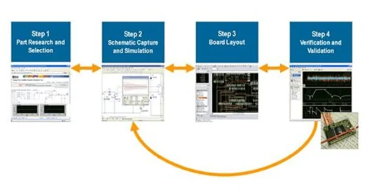
The 4-Stage PCB Prototyping Workflow
1. Research & Component Selection
The foundation of any successful PCB design for export markets begins with strategic component selection. Engineers should consider:
- Global semiconductor suppliers (TI, NXP, Analog Devices)
- Component availability for international supply chains
- Compliance with target market regulations (CE, RoHS, REACH)
- Cost-effective alternatives without compromising quality
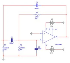
2. Schematic Capture and Circuit Simulation
This phase transforms conceptual designs into workable circuit diagrams. For businesses seeking quick turn PCB fabrication, proper schematic development is essential. Key tools include:
- SPICE-based simulation software (PSpice, HSpice)
- Industry-standard EDA tools (Altium, Eagle, KiCad)
- Virtual testing environments for export compliance verification
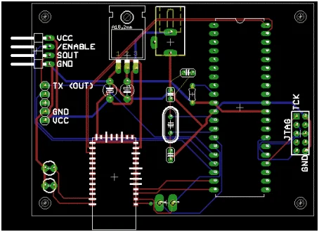
3. PCB Layout and Design Optimization
The transition from schematic to physical board requires careful consideration of:
- Optimal component placement for manufacturing efficiency
- Signal integrity in high-speed designs
- Thermal management for reliable operation
- Design for manufacturability (DFM) principles
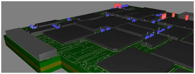
4. Verification & Functional Testing
Before moving to mass PCB production for export, rigorous testing ensures:
- Electrical performance meets specifications
- Design complies with international standards
- Reliability under expected operating conditions
- Compatibility with automated assembly processes
From Prototype to Production: Scaling Your PCB Design
Successful prototyping leads to the product development phase, where considerations shift to:
- Design for cost-effective mass production
- Supply chain optimization for global distribution
- Quality control systems for export markets
- Packaging and logistics requirements
Choosing the Right PCB Prototyping Partner
For businesses looking for reliable PCB manufacturers in China, consider these factors:
- Experience with your specific industry applications
- Capability to scale from prototype to full production
- International certifications and quality standards
- Turnaround time for prototyping iterations
Future Trends in PCB Prototyping Technology
The PCB prototyping industry is evolving with:
- AI-assisted design optimization
- Advanced materials for high-frequency applications
- 3D printing for rapid prototyping
- IoT-focused design methodologies
By mastering the PCB prototyping workflow, electronics manufacturers can significantly improve their competitiveness in global markets while reducing development risks and costs.


