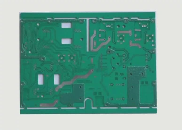
Essential PCB Layout and Wiring Guidelines for Optimal Circuit Board Design
When designing printed circuit boards for international export, following industry-standard layout principles ensures reliable performance and manufacturability. These PCB design best practices are crucial for electronic manufacturers in China serving global markets.
Strategic Component Placement for Efficient PCB Assembly
How to arrange components on a PCB for maximum efficiency:
- Module-based organization: Group related circuits by function, maintaining proximity within each module
- Separation of analog/digital: Keep analog and digital circuits physically separated to prevent interference
- Clearance requirements: Maintain 1.27mm from positioning holes and 3.5-4mm from screw mounting holes
Critical Spacing Considerations for Reliable PCB Manufacturing
For high-quality PCB production in China, observe these spacing rules:
- 5mm minimum from board edges for all components
- 2mm spacing between adjacent component pads
- No vias under horizontal resistors, inductors, or electrolytic capacitors
- 2mm clearance around metal-shell components
Thermal Management and Power Distribution Best Practices
PCB thermal design solutions for optimal performance:
- Distribute high-heat components evenly across the board
- Keep heat sources away from sensitive components and traces
- Place power sockets strategically around the board perimeter
- Maintain proper spacing for power plug insertion/removal
Professional Wiring Techniques for Signal Integrity
How to route PCB traces properly for clean signal transmission:
- Power traces: Minimum 18mil width
- Signal traces: Minimum 12mil width (8-10mil for CPU I/O)
- 10mil minimum spacing between traces
- Radial routing for power/ground, avoiding signal loops
Via and Pad Specifications for Manufacturing Reliability
Follow these PCB manufacturing standards for via and pad design:
- Minimum 30mil via diameter
- DIP components: 60mil pads with 40mil holes
- SMD resistors (0805): 51×55mil pads
- Non-polar capacitors (0805): 50mil pads with 28mil holes
“Proper PCB layout and wiring techniques are fundamental to producing reliable circuit boards that meet international quality standards for export markets.”
Additional Design Considerations for Export-Quality PCBs
For global PCB sourcing requirements, remember to:
- Maintain uniform component orientation and polarity markings
- Use copper pour in low-density areas (mesh >8mil/0.2mm)
- Avoid through-holes on SMD pads to prevent solder issues
- Keep critical signals away from connector pins
By implementing these PCB design guidelines for manufacturers, you’ll create boards that meet the rigorous demands of international electronics trade while optimizing for manufacturability and reliability.

