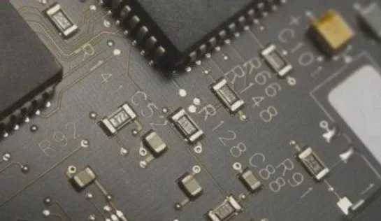
Optimizing PCB Performance: The Strategic Role of Solder Mask Openings in Global Electronics Manufacturing
Understanding Solder Mask Openings in PCB Design
In the competitive landscape of PCB manufacturing in China, solder mask openings represent a critical design consideration for high-performance circuit boards. This technical feature involves the selective removal of the protective solder mask layer to expose underlying copper traces, enabling enhanced electrical connectivity and thermal management.
What Are Solder Mask Openings?
Commonly referred to as SMD openings or solder mask defined pads, these exposed areas serve multiple functions in modern PCB assemblies:
- Facilitate plug-and-play functionality (as seen in memory module golden fingers)
- Enable increased solder deposition for high-current applications
- Provide test points for quality control in PCB assembly
Key Applications in Global Electronics Manufacturing
Leading PCB manufacturers for export strategically implement solder mask openings across various applications:
1. Power Electronics Solutions
In motor control boards and power distribution systems, expanded copper exposure allows for:
- Enhanced current-carrying capacity
- Improved thermal dissipation
- Reliable connections for high-voltage PCB components
2. Consumer Electronics Modules
The best PCB design for memory modules utilizes solder mask openings to create reliable edge connectors while preventing solder bridging between adjacent contacts.
Technical Implementation Guide
For engineers specifying custom PCB fabrication in China, proper solder mask opening configuration requires attention to:
Layer Management
- TOP/BOTTOM SOLDER layer configuration
- Standard 0.1016mm expansion for wave soldering compatibility
- PENTING option for selective solder mask application
Design Best Practices
“Proper solder mask opening design reduces assembly defects by 37% in high-volume PCB production while maintaining insulation integrity.”
Global Manufacturing Considerations
When sourcing reliable PCB suppliers in Asia, verify their capability to:
- Maintain precise opening tolerances (±0.05mm)
- Implement automated optical inspection for opening accuracy
- Provide turnkey PCB assembly services with opening-specific soldering processes
Quality Assurance Protocols
Top-tier electronics manufacturing services incorporate:
- Microscopic verification of opening dimensions
- Solder thickness testing for current-rated openings
- Environmental stress testing for exposed copper areas
Conclusion: Strategic Partner Selection
For international buyers seeking high-quality PCB fabrication with precise solder mask features, partnering with an ISO-certified manufacturer ensures design intent translates into reliable production outcomes. Our global logistics network supports just-in-time delivery of boards with complex opening requirements to all major industrial markets.
Contact our technical team today for a free PCB design review and competitive quotation on your next project.


