Understanding PCB Back Drilling: A Complete Guide for High-Frequency Electronics
In the world of high-performance PCB manufacturing, back drilling has emerged as a critical signal integrity solution for multilayer boards. Also known as controlled-depth drilling or secondary drilling, this specialized process addresses the challenges of high-speed signal transmission in complex circuit designs.
What Is PCB Back Drilling Technology?
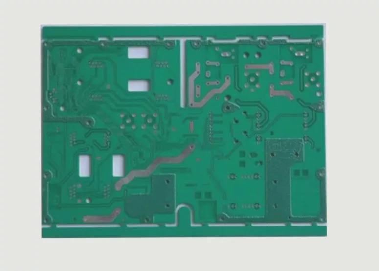
Back drilling is a precision manufacturing technique used in the production of multilayer PCBs, particularly those with 8+ layers like the 14-layer boards shown above. When connecting internal layers (for example, layer 6 to layer 10), traditional through-hole drilling creates unwanted connections called stubs that extend to all layers.
“These stubs act like miniature antennas, causing signal reflections and degrading performance in high-frequency applications. Back drilling removes these unnecessary connections while preserving the required circuit pathways.”
Key Advantages of Back Drilling for Export-Quality PCBs
- Reduces signal interference noise by up to 40% in high-frequency applications
- Enhances signal integrity for better data transmission in communication equipment
- Lowers overall PCB thickness and weight – crucial for aerospace applications
- Reduces reliance on complex blind/buried vias, simplifying production
- Improves impedance matching for high-speed digital circuits
How Professional PCB Manufacturers Implement Back Drilling
Leading PCB manufacturers in China follow this precise workflow for export-grade back drilling:
- Initial drilling: Using positioning holes for perfect alignment of through-holes
- Electroplating preparation: Dry film sealing protects critical areas during copper plating
- Outer layer patterning: Creating the circuit layout before back drilling
- Precision back drilling: Specialized drill bits remove stub portions with ±0.05mm tolerance
- Post-drill cleaning: Ensures no residual copper fragments remain in holes
Technical Specifications of Back Drilled PCBs
- Typical applications: 8-50 layer boards for high-frequency use
- Standard thickness: 2.5mm or greater for backplane applications
- Large aspect ratio (up to 15:1) capability
- Minimum initial hole diameter: 0.3mm standard
- Back drill size: Typically 0.2mm larger than target hole
- Stub length (B value): Controlled within 50-150μm range
Industry Applications of Back Drilling Technology
This advanced PCB manufacturing technique is essential for:
- 5G communication equipment and network infrastructure
- Enterprise-level servers and data center hardware
- Medical imaging and diagnostic electronics
- Military radar and avionics systems
- Aerospace and satellite communication systems
Why Choose Chinese PCB Manufacturers for Back Drilling?
China has become the global leader in high-tech PCB manufacturing, offering:
- Advanced back drilling equipment with micron-level precision
- Cost-effective solutions for high-volume production
- Military-grade manufacturing capabilities for sensitive applications
- Complete supply chain for quick turnaround times
- ISO-certified quality control processes
For international buyers looking for reliable PCB back drilling services, partnering with an experienced Chinese PCB manufacturer ensures you get the perfect balance of performance, quality, and value for your high-frequency electronic applications.