PCB Circuit Design and Production Process
1. Original Manuscript Creation
- The circuit diagram is designed and printed onto transparent film or translucent sulphate paper using a laser (inkjet) printer.
- Attention Points:
- Ensure mirror printing is selected to reveal the copper surface during development.
- Connect the circuit diagram ink surface closely with the green photosensitive film for high resolution.
- Keep the draft surface clean and free of dirt.
2. Exposure Process
- Expose the printed circuit diagram onto the photosensitive film surface using a 20W lamp or sunlight.
- Double Panel Exposure Method:
- Align and drill positioning holes for accurate exposure.
- Fix the manuscript on both sides with adhesive paper for a clear image.
3. Imaging and Development
- Prepare imaging agent by mixing imaging agent powder with water.
- Develop the photosensitive plate until the copper foil is clear.
- Rinse with water and dry the plate carefully.
- Points to Consider:
- Proper proportion of imaging agent and water is crucial for development.
- Do not reuse the development fluid to prevent overdevelopment.
- Take precautions to avoid scratching the film surface.
4. Etching Process
- Prepare Ferric Chloride Etching Solution by mixing ferric chloride with water.
- Etch the PCB to create fine lines for circuit connections.
PCB Etching Process
- Plastic Basin: Etching time is approximately 5 to 15 minutes. It is recommended to gently shake the plastic basin during etching.
- Etching Machine: When using a new solution, the etching time is around 1.5 to 3 minutes. Ensure that thin lines less than 0.5mm are etched.
- Rinse.
- Dry.
Important Points to Note:
- Handle the film surface with care to avoid damage.
- Dip the plate in the etching solution for about 2 seconds, then inspect for successful development. To address underdevelopment, if copper foil in non-circuit areas turns pink, rinse the product with water before redeveloping in the development solution (adjust development time accordingly).
- Photosensitive film can be welded directly without removal. If removal is necessary, solvents such as alcohol and acetone can be used.
- The thickness of the etching solution affects the process speed.
The schematic below illustrates the board fabrication process.
Fabrication Tips:
Fabricating the plate is simple. The mentioned times are for reference only; actual testing is crucial. Conduct tests with a few small plates to gauge proficiency; typically, one or two tests are sufficient. Once mastered, the quality of your produced circuit boards will rival or exceed that of professional PCB manufacturers.
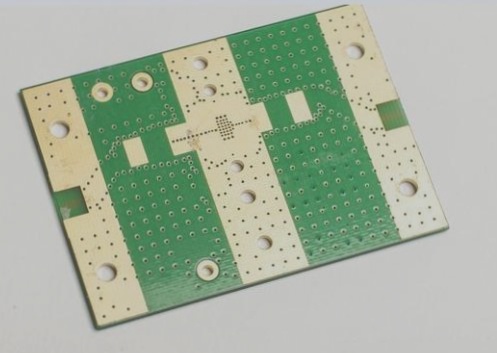
Photosensitive Plates for Electronics
Photosensitive plates are ideal for electronic enthusiasts, students, and engineers in the electronic research, development, and testing fields. These plates enable convenient production without the need for specialized equipment. Refer to the production method instructions for details.
Key Features:
- Standard size: 100mm × 150mm single-sided electric board
- Uniform photosensitive film
- Quick exposure and easy development result judgment
- High success rate and user-friendliness
- Cost-effective and high confidentiality
Price: 10 yuan per tablet, including one package of developer (imaging five standard 100mm × 150mm plates). Bulk purchase discounts available.
Photosensitive circuit boards, also known as photosensitive PCBs, involve coating a circuit board evenly with photosensitive film. The film dissolves where light strikes, leaving the copper skin intact on the board, resistant to ferric chloride corrosion.
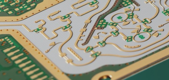
High-precision base circuit boards can be corroded with special corrosives at 0.2mm/0.1mm, achieving precise line widths and spacings for intricate designs.